Without the use of solvents, researchers from the MESA+ Institute at the University of Twente, Riga Technical University, and the Department of Chemical Engineering at the Vrije Universiteit Brussel have managed to arrange extremely small particles (10 µm to 500 nm, 10 to 100 times thinner than a human hair) in a thin layer.
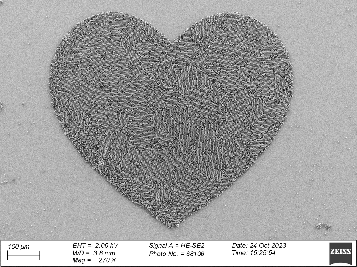 AFM image of microparticles controlledly printed in the shape of a heart icon. The scale is 100 µm, which is a hair thickness. Image Credit: Ignaas Jimidar
Common methods based on crystallising solutions are not as versatile as we would like. What’s more, previous dry methods were mainly effective on sticky surfaces, which limited their applications.
Ignaas Jimidar, Postdoctoral Researcher, University of Twente
The group came up with a way to connect the particles to hard, non-stick surfaces to solve this problem. After manually rubbing the particles over the surface, they were able to create a single layer of closely spaced particles in the shape of a hexagon in around 20 seconds.
The rubbing is done using a stamp made of a silicone-like material called PDM. The static electricity generated by the rubbing process, especially on harder surfaces, and the forces between the particles and the surface are crucial for creating the desired patterns. We encounter this static electricity in everyday life, if we rub a balloon against our hair or feel a shock on a dry winter day when we touch a metal object.
Kai Sotthewes, Assistant Professor, University of Twente
Andris Šutka of Riga Technical University added, “The pattern-making process worked on both conductive and non-conductive surfaces, and the best results were achieved with certain types of particle powders, such as polystyrene (used as insulation) and polymethyl methacrylate or PMMA, also known as Plexiglas.”
The ubiquitous silicon used in modern electronics functioned best on surfaces coated with fluorocarbon, a kind of Teflon coating, and in an environment devoid of humidity.
Silica particles are therefore slightly less user-friendly, but they are resistant to all kinds of solvents, which makes them suitable for biological and chemical analysis and detection techniques.
Gijs Roozendaal, University of Twente
Jimidar added, “We eventually succeeded in creating a series of microscopic patterns and logos on ‘wafers’ on a large scale, and visualized them all using an atomic force microscope. This represents a promising development for improving electronics, detecting all kinds of chemical and biological substances, and even detecting counterfeit goods. The last is possible because particles in certain patterns refract light differently depending on the angle. So you could detect colors using these microparticles.”
The study will be featured on the print edition’s cover and published in the journal ACS Applied Materials & Interfaces.
Journal Reference:
Sotthewes, K., et. al. (2024) Toward the Assembly of 2D Tunable Crystal Patterns of Spherical Colloids on a Wafer-Scale. ACS Applied Materials & Interfaces. doi:10.1021/acsami.3c16830.
Source: http://www.vub.ac.be/