LayTec is expanding the application of its sensors to new fields, one of which is growth of oxides on silicon. In collaboration with Dr. Lutz Geelhaar from Namlab in Dresden (Germany) – a joint venture of Qimonda and TU Dresden – first promising in-situ measurement results have been gained. Dr. Steffen Uredat from LayTec will present the method at the SVC Conference in Chicago (USA) in April.
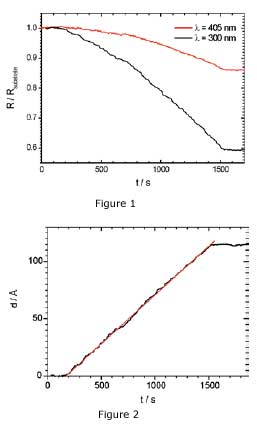 Fig. 1: Deposition of 115 Å ZrO2 on TiN coated Si, monitored by reflectance measurements at wavelengths of 300 and 405 nm.<br>
Fig. 2: Thickness of the ZrO2 layer on TiN coated Si determined by insitu reflectance measurement at 300 nm (black curve).
Fig. 1: Deposition of 115 Å ZrO2 on TiN coated Si, monitored by reflectance measurements at wavelengths of 300 and 405 nm.<br>
Fig. 2: Thickness of the ZrO2 layer on TiN coated Si determined by insitu reflectance measurement at 300 nm (black curve).
In this work LayTec will demonstrate how reflectivity measurements at optimised UV wavelength can be used to monitor the deposition of extremely thin ZrO2 and Al2O3 layers (down to 30 Å) on silicon in MBE. The accuracy of this method was shown to be up to ±2.5 Å for 50 Å ZrO2 layers. Fig. 1 shows the reflectance signals at wavelengths of 300 and 405 nm as measured during the deposition of 115 Å ZrO2 on Si, which had previously been coated by 46 Å TiN. The reflectance decreases with increasing thickness of the oxide layer. For ultra-thin layers, the 300 nm signal is most sensitive to changes in layer thickness.
However, when thicker layers are grown, the 300 nm signal passes a Fabry-Perot minimum. In this case LayTec‘s doublewavelength set-up provides the second wavelength to close the gap. In the case of oxides, additional 405 nm reflectance allows to expand the effective range of measurements to all typical thicknesses between 30 Å and 500 Å.
If the refractive index and the absorption coefficient of the oxide layer are well known, the layer thickness can be calculated directly from the measured reflectance. Fig. 2 shows the change of the thickness of a 115 Å layer of ZrO2 as obtained from the 300 nm reflectance measurement, revealing a fairly linear growth with a growth rate of 0.085 Å/s, as indicated by the straight red line in the figure.
Beyond growth rate studies, reflectance measurements at longer wavelengths were used to determine the wafer temperature based on a double wavelength band-edge approach. It was found out that during oxide growth the wafers experience a temperature offset of 20°C between process temperature and the wafer surface temperature, which is attributed to heating effects from the hot MBE sources.
This work opens a new field of application for LayTec tools not only in MBE but also in sputter and other thin-film techniques.