Since the invention of atomic force microscopy (AFM)1, it has had widespread application in non-destructive sample surface imaging and significant interest in its magnetic, electrical, and mechanical properties.
Yet, in addition to those, AFM provides huge potential for local surface modification and patterning, utilizing either ferroelectric switching, excessive cantilever loading force resulting in mechanical scratching, or by oxidizing the surface via the application of AFM tip bias.
Also known as ‘bias mode AFM nanolithography,’ local oxidation has been widely utilized in the customization of nanoscale conducting or semiconducting surface patterning2, 3.
Bias mode AFM nanolithography supplies numerous benefits for customized patterning: it circumvents the diffraction limit present in optical lithography techniques, its procedure is straightforward and it does not need optical masks.
The tip-sample contact region forms an oxidized layer (Figure 1) by applying a voltage bias between a substrate and a conductive AFM tip. Nanopattern control by oxidation happens by manipulating experimental parameters, including the applied AFM tip bias, the tip material/geometry, humidity, and scan speed.
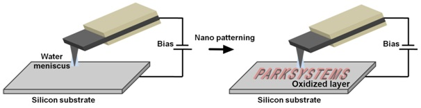
Figure 1. Schematic representation of bias-assisted AFM nanolithography via local surface oxidation. Patterns are created on the surface by oxidation upon bias application between tip and sample.
In this article, nanopatterning via oxide growth on a bare silicon wafer4 using bias mode AFM nanolithography with Park SmartLitho is discussed. This is the new nanolithography software developed by Park Systems5.
In addition, the capabilities of Park SmartLitho for lithography on ferroelectric samples is demonstrated by patterning local domains of a PZT (lead zirconium titanate) film on silicon wafers6.
Complex structures with detailed and elaborate features were fabricated using Park SmartLitho via both oxidation and ferroelectric domain switching. Lastly, optimized process parameters for successful nanopatterning are proposed.
The software is perfectly suited for investigations into ever-decreasing feature sizes and line spacings for advanced nanoelectronics and for novel device surface structure development based on nanolithography.
Methods and Materials
To show nanopatterning via oxidation and ferroelectric domain switching, a bare silicon wafer and a PZT film on a silicon wafer were used respectively. So that the height contrast between the oxidized layer and the substrate could be identified, the root mean square roughness (Rq) for the bare silicon wafer was > 1 nm.
A CDT-NCHR cantilever with a nominal spring constant of 80 N/m and a resonance frequency of 400 kHz was utilized for oxidation nanopatterning. The CDT-NCHR tip contains a conductive diamond coating (< 10 kOhm at the platinum surface) and the tip curvature radius was 100 nm ~ 200 nm.
The tip radius of the CDT-NCHR was a little larger than tips with other conductive metal coatings; yet, diamond coated tips exhibit higher sensitivity and improved operational stability.
A PPP-EFM cantilever with a nominal spring constant of k = 2.8 N/m and a resonance frequency of 75 kHz was used For nanopatterning via ferroelectric domain switching on a PZT.
The PPP-EFM tip has a platinum-iridium coating and a radius of approximately 25 nm. A soft conductive cantilever was used since the ferroelectric domain switching on PZT does not need a high loading force between the AFM tip and the sample surface. The detailed scan parameters can be seen in Table 1.
Table 1. AFM nanolithography parameters.
| |
Nanopatterning by oxidation |
Nanopatterning by Ferroelectric domain switching |
| Sample |
Bare Silicon wafer |
PZT on Silicon wafer |
| Cantilever |
CDT-NCHR |
PPP-EFM |
| Environment |
High humidity (> 60%) |
Ambient |
| |
Nanolithography |
AFM image |
Nanolithography |
AFM image |
| Scan size |
35 μm x 35 μm |
40 μm x 40 μm |
30 μm x 15 μm |
35 μm x 25 μm |
| Pixel resolution |
400x400 |
1024x1024 |
300x300 |
1024x1024 |
| Scan rate |
20 μm/s |
0.5 Hz |
10 μm/s |
0.5 Hz |
| Bias range |
0 ~ –10V |
- |
0 ~ –10 V |
AC bias: 2V
DC bias: 0V |
All of the measurements were performed on a Park NX10 AFM system using the new AFM nanolithography software from Park Systems, Park SmartLitho. Park SmartLitho combines a number of nanolithography modes, including constant force mode, constant Z scanner mode, bias (and other) modes with a user-friendly graphic editor.
The user is able to access a variety of template types for customized nanopatterning such as polygons, bitmap images, polydots, and polylines.
Park SmartLitho is available either as a stand-alone version or embedded in the Park SmartScan™ operating software, as seen in Figure 2. The stand-alone and embedded versions supply the same functions, like drawing file creation in addition to bitmap or pattern editing, and can operate the user’s chosen/preferred nanolithography mode.
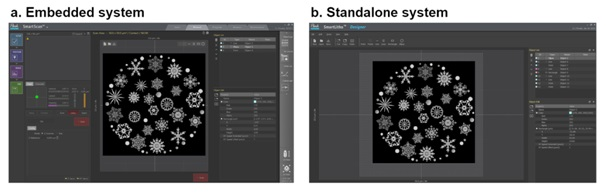
Figure 2. Captured images of Park SmartLitho software, (a) embedded in Park SmartScan imaging software, and (b) the stand-alone version.
Results and Discussion
The original bitmap image which is utilized as the nanopatterning template, plus the height and corresponding 3D images of the sample surface after bias mode AFM nanolithography are shown in figure 3.
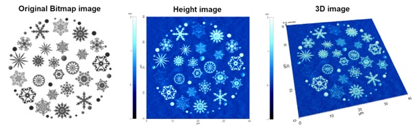
Figure 3. Original bitmap image used as the template (left), AFM height image after bias assisted AFM nanolithography (center), and corresponding 3D image of the sample surface (right). The nanopatterning was generated by surface oxidation.
The nanopattern on the surface of the bare silicon wafer closely resembled the template of the Christmas ball. The pattern was produced using bias assisted silicon oxidation by applying a sufficiently high voltage between the sample and tip.
The oxide layer thickness was controlled by the applied bias magnitude and environmental humidity. The oxide layer thickness was directly proportional to the applied tip bias. In addition, oxidation needed a water meniscus at the AFM tip end that was affected by environmental humidity7.
So, the measurement was performed from a 0 V ~ 10 V tip bias under high humidity conditions (> 60 %). The oxide nanopattern featured heights that ranged from 0.8 nm ~ 1.5 nm. Two of the constituent structures (5 μmx5 μm) with their corresponding 3D images and line profile information are shown in Figure 4.
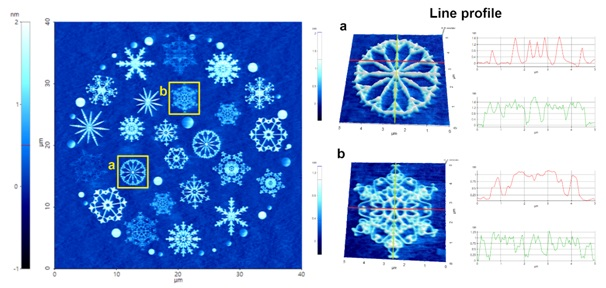
Figure 4. AFM height images after nanolithography and line profile analysis on two of the constituent structures. AFM line profiles in a and b show the ~1 nm height of the oxide layer from the substrate.
Structure heights of approximately 1 nm were determined from these line profiles. The distinct height image contrast after nanolithography showed the successful and high-resolution nanopatterning available by bias assisted oxidation via the new Park SmartLitho software from Park Systems.
Height and piezoelectric force microscopy (PFM) quad images, their line profile information, and 3D images after lithography are shown in Figure 5. By applying different biases between the tip and sample ferroelectric domains in PZT can be switched.
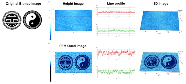
Figure 5. Original bitmap images used as templates (left), AFM height and PFM quad images after ferroelectric switching in AFM nanolithography bias mode, line profile analysis (center), and the corresponding 3D images (right). The nanopattern on PZT was generated by ferroelectric domain switching.
Both AFM non-contact imaging for height information and PFM imaging for PFM quad information were performed after bias mode AFM nanolithography. The height images were flat surfaces without a pattern, as shown in both.
Yet, the structure resolved in the PFM quad strongly resembled the original traditional Korean pattern template, showing successful ferroelectric domain switching.
Nanopatterning via ferroelectric switching needs slow scan speeds and lower loading force scanning to avoid sample damage due to contact mode, while nanopatterning by oxidation requires humidity control for high-quality nanolithography.
Conclusion
In this article, the nanopatterning via oxide growth on a bare silicon wafer utilizing bias mode AFM nanolithography with Park SmartLitho is outlined, a novel nanolithography software from Park Systems on a Park NX10 AFM system.
Park SmartLitho, a bias assisted nanopatterning of complicated structures can be readily performed by locally oxidizing the surface of a silicon wafer and switching ferroelectric domains of a PZT film.
In addition, optimized parameters were proposed. These included a tip bias range, humidity values, scan rate and suitable cantilevers to produce accurate and distinct nanoscale oxide patterns on a silicon substrate as well as ferroelectric domain patterns on PZT.
This study shows that nanopatterning by AFM nanolithography, especially oxidation patterning on silicon substrates and Park SmartLitho, supplies significant potential for customized nanosensor surface modification, in addition to nanodevices for semiconductor research and industry.
References and Further Reading
- Binnig, G., Quate, C. F., & Gerber, C., Atomic force microscope. Physical review letters, 56 (9) (1986) 930.
- Minne, S. C., Flueckiger, P., Soh, H. T., & Quate, C. F., Atomic force microscope lithography using amorphous silicon as a resist and advances in parallel operation. Journal of Vacuum Science & Technology B: Microelectronics and Nanometer Structures Processing, Measurement, and Phenomena, 13 (3) (1995) 1380-1385.
- Garcia, R., Martinez, R. V., & Martinez, J., Nano-chemistry and scanning probe nanolithographies. Chemical Society Reviews, 35 (1) (2006) 29-38.
- Garcı́a, R., Calleja, M., & Pérez-Murano, F., Local oxidation of silicon surfaces by dynamic force microscopy: Nanofabrication and water bridge formation. Applied Physics Letters, 72 (18) (1998) 2295-2297.
- Advanced Vector Nanolithography Using Closed Loop Scan System (2010, Online Article). Retrieved from: https://www.parksystems.com/kr/learning-center/lc-detail.learning133
- Li, D., & Bonnell, D. A., Ferroelectric lithography. Ceramics International, 34 (1) (2008) 157-164.
- Abdullah, A. M., Hutagalung, S. D., & Lockman, Z., Influence of room humidity on the formation of nanoscale silicon oxide patterned by AFM lithography. International Journal of Nanoscience, 9 (04) (2010) 251-255.
This information has been sourced, reviewed and adapted from materials provided by Park Systems.
For more information on this source, please visit Park Systems.