Thin films are layered structures ranging from a single atomic or molecular monolayer to several microns thick. These structures form naturally, such as the self-limiting oxide layer that develops on aluminum, providing resistance to further oxidation, and are also deliberately deposited for a wide variety of engineering applications.
Among the earliest industrial applications of thin-film technology was depositing zinc coatings on iron and steel to prevent corrosion, paving the way for the far more precise film-deposition processes used in today’s manufacturing.
Two industries where thin films play a critical role are optical component manufacturing and semiconductor device fabrication. In semiconductor processing, integrated circuits are built through sequential deposition and etching of conductive, semiconductive, and insulating material layers.1
In optical component fabrication, thin films serve as protective, anti-reflective, and reflective coatings, achieving the desired optical response through the combined effect of multiple layers with differing refractive indices.2
Because device performance in both domains relies heavily on layer thickness, consistent production requires accurate, non-destructive film thickness measurements, increasingly at submicron spatial resolution.
Theoretical Background: Optical Interference Methods
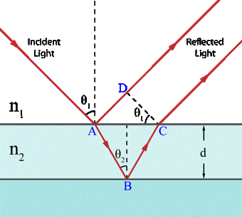
Figure 1. Schematic of light rays reflecting from the upper and lower boundary interfaces of a thin film. Image Credit: Public domain, Wikipedia
Optical interference is the most popular non-contact technique for determining thin-film thickness.3 Illuminating a film-coated sample with a broadband light source produces partial reflections of incident light at the upper (air–film) and lower (film–substrate) interfaces of the film, as depicted schematically in Figure 1.
The two reflected wavefronts recombine and interfere to generate a reflectance spectrum, which can be described using the Fresnel equations that govern reflection and transmission at each interface.
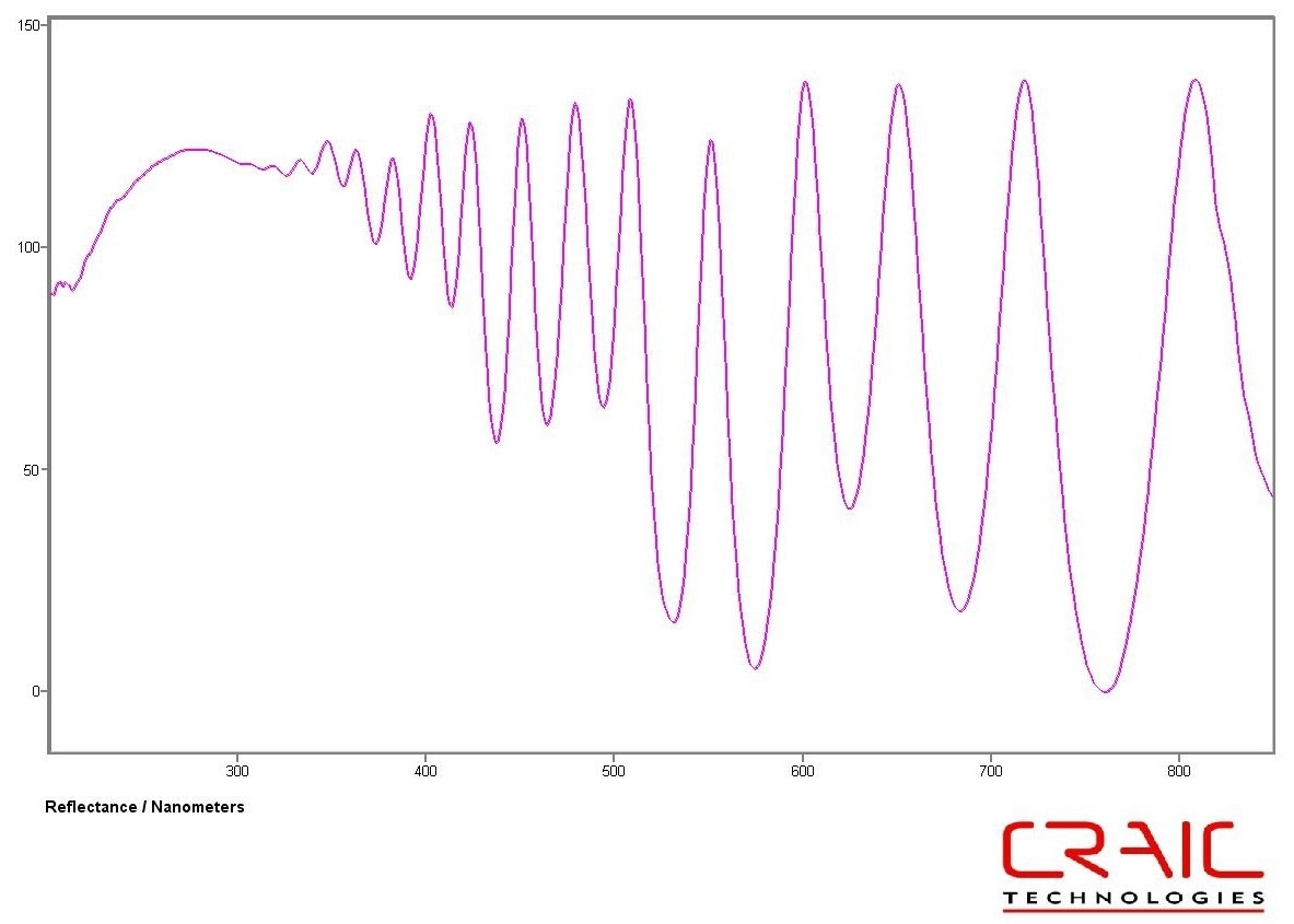
Figure 2. Interference spectrum acquired from a thin film using a microspectrophotometer. Image Credit: CRAIC Technologies
The degree of constructive or destructive interference at any specific wavelength depends on the optical path difference between the two reflected rays. This optical path difference is a function of the film's refractive index, the wavelength of the incident light, the angle of incidence, and, most importantly, the film thickness.
Under white-light illumination, this wavelength-dependent interference creates the familiar multicolored banding observed in thin films such as oil on water.
By recording the reflectance (or transmittance) intensity as a function of wavelength, the microspectrophotometer quantifies this effect, producing an interference spectrum such as the one illustrated in Figure 2. Fitting the measured spectrum to an optical model of the film stack, incorporating estimated or known optical constants for every layer, allows film thickness to be determined with high accuracy.
Instrumentation and Measurement Approach
Microspectrophotometry provides multiple benefits that make it especially ideal for film-thickness metrology in manufacturing and research environments:
- Non-contact measurement: The sample is not physically probed, reducing the likelihood of damage or contamination
- Speed: Measurement acquisition is sufficiently quick to be conducted in-line during production
- Flexibility: A single instrument can characterize films covering a broad range of thicknesses and material types
- Substrate versatility: Instruments can be set up to record either reflected or transmitted spectra, allowing for measurement on both opaque and transparent substrates
- Multilayer capability: Stacks composed of multiple distinct films can be modeled and resolved concurrently
- Spatial resolution: Measurements can be restricted to microscopic sample regions, accommodating both point measurements on individual device features and spatially resolved thickness mapping across a sample
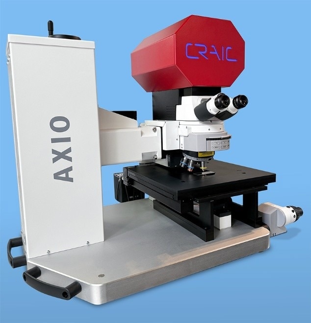
Figure 3. 2030XL PRO™ microspectrophotometer designed to measure thin film thickness of wafers over 300 mm in diameter. Image Credit: CRAIC Technologies
This last capability is particularly valuable for contemporary integrated circuits, where film thicknesses are typically on the order of tens of nanometers whereas circuit feature dimensions fall in the submicron range.
CRAIC Technologies’ instruments meet these demands by integrating a spectrophotometer with a microscope, a permanently calibrated, variable sampling aperture, and software for automated data collection and evaluation (Figure 3).
Through this configuration, the sampled region can be reduced from more than 100 microns to well under a single micron in diameter, allowing film-thickness measurements to be localized to individual submicron device structures.
By supporting both reflectance and transmittance modes, as well as opaque and transparent substrates, these systems serve semiconductor wafers, flat-panel display substrates, and microelectromechanical systems (MEMS) alike.
Representative Application: Silicon Dioxide Films on Silicon
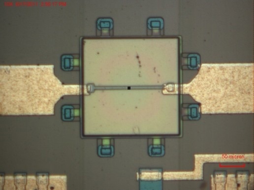
Figure 4. Integrated circuit imaged through a CRAIC Technologies microspectrophotometer; the black square denotes the entrance aperture defining the sampled area. Image Credit: CRAIC Technologies
Measurements conducted on integrated-circuit test structures with a CRAIC Technologies microspectrophotometer highlight the practical execution of this method. Figure 4 illustrates the instrument's field of view, with the entrance aperture (the area from which the spectrum is collected) shown as a defined sampling region overlaid on the circuit image.
The system measures light acquired through this aperture as intensity versus wavelength, producing an interference spectrum analogous in origin to that of Figure 2, but obtained from a sampling region confined to a single submicron circuit feature.
Figure 5 displays reflectance spectra collected from three silicon dioxide films of varying thicknesses, each deposited onto a silicon substrate. FilmPro™ modeling software was used to analyze the spectra. This software fits the measured interference pattern to an optical model of the SiO2/Si system to extract film thickness.
The resulting thicknesses for the three samples were 10.1 nm, 30.0 nm, and 50.0 nm, corresponding to the red, blue, and green spectra, respectively. The systematic shift in interference peak position with increasing film thickness correlates with the theoretical relationship outlined in Section 2, in which optical path length, and consequently phase difference, scales with film thickness.
This example shows that the same foundational interference-based approach utilized for macroscopic optical coatings is applicable, when proper instrumentation is used, for films just tens of nanometers thick and sampling regions below one micron across – a spatial and thickness regime essential for semiconductor process control.
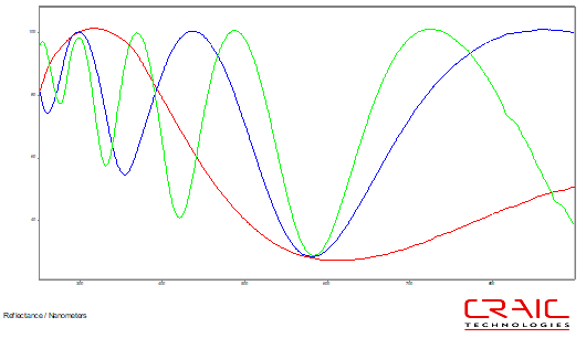
Figure 5. Reflectance interference spectra for three silicon dioxide films of differing thickness (10.1 nm, 30.0 nm, and 50.0 nm) deposited on a silicon substrate, modeled using FilmPro™ software. Image Credit: CRAIC Technologies
Conclusion
Optical interference-based microspectrophotometry offers a non-destructive, rapid, and spatially resolved technique for thin-film thickness measurements across a wide spectrum of materials, substrates, and length scales.
The underlying physics–dictated by the Fresnel equations and the wavelength-dependent phase relationship between reflections at the film's upper and lower boundaries–is thoroughly established. Ongoing developments in instrumentation and modeling software have broadened the method's practical resolution to submicron sampling regions and nanometer-scale film thicknesses.
Measurements of 10.1 nm, 30.0 nm, and 50.0 nm silicon dioxide films illustrate the power of microspectrophotometry as a metrology tool ideally suited to the dimensional requirements of today’s semiconductor devices, flat-panel displays, and MEMS production.
References and Further Reading
- Van Zant, Peter. Microchip Fabrication, 4th Edition. London, UK: McGraw-Hill, 2000
- Heavens, Oliver S. Optical Properties of Thin Solid Films. New York: Dover Publications, 1965
- Pliskin, W. A. "Nondestructive Optical Techniques for Thin-Film Thickness Measurements," in Physical Measurements and Analysis of Thin Films, E. M. Murt and W. G. Guldner, Eds. New York: Plenum, 1969, Chap. 1
- Martin, Paul. "Thin Film Thickness Measurements of Sub-micron Sample Areas." CRAIC Technologies, Inc., 2009

This information has been sourced, reviewed, and adapted from materials provided by CRAIC Technologies.
For more information on this source, please visit CRAIC Technologies.