The NMT04 NanoMechanical Testing System represents the cutting edge of in-situ SEM/FIB nanoindentation technology. Leveraging FemtoTools' proprietary MEMS technology, it offers unparalleled precision for analyzing materials at the micro- and nanoscale.
The NMT04 features MEMS-based force sensors that deliver exceptional resolution, repeatability, and dynamic response. This system is perfectly suited for the nanoindentation of metals, ceramics, thin films, and micro-scale structures such as metamaterials and MEMS. It also includes expandable capabilities through accessories, catering to various research domains.
It is highly effective in areas such as micro-compression testing, tensile testing of thin films or nanowires, and fracture testing of microbeams. This allows for accurate measurement of plastic deformation, crack propagation, and fracture toughness. Its compact structure is compatible with the majority of commercial SEMs, facilitating thorough correlative analysis alongside methods such as EBSD and EDX.
Key Features
Unmatched Dynamic Range
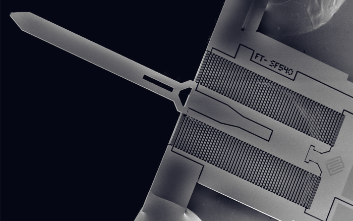
Image Credit: Oxford Instruments Materials Science
Micro-Electro-Mechanical System (MEMS)-based force sensors exhibit an unparalleled dynamic range of up to 100 kHz, attributed to their remarkably small mobile mass and elevated stiffness. Additionally, the precise fabrication tolerances of MEMS facilitate the attainment of the lowest achievable noise floor, which can reach as low as 500 pN.
Resonance frequency: up to 100 kHz
Force noise floor: down to 500 pN
True Displacement Control
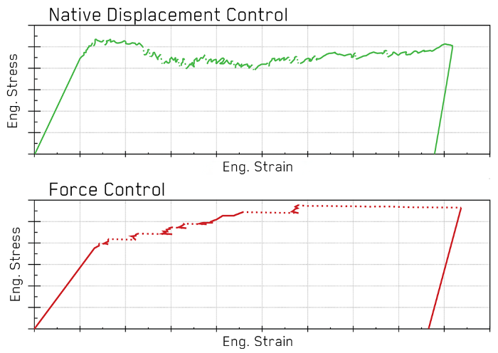
Image Credit: Oxford Instruments Materials Science
Displacement-controlled nanoindentation is crucial for assessing and contrasting mechanical properties at uniform indentation depths, thereby guaranteeing the examination of comparable material volumes.
Control mode: Inherently Displacement Controlled
Open Measurement Frame
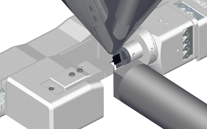
Image Credit: Oxford Instruments Materials Science
The NMT04 has been specifically engineered to function harmoniously with Electron Backscatter Diffraction (EBSD) or Scanning Transmission Electron Microscopy (STEM) detectors within the SEM. Its open measurement frame allows for concurrent observation and analysis of the microstructural evolution of the sample throughout mechanical testing.
Accessories
High-Temperature Module
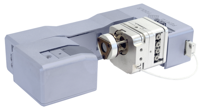
Image Credit: Oxford Instruments Materials Science
The high-temperature module facilitates mechanical testing, including nanoindentation, micro-pillar compression, micro-cantilever bending, and micro-tensile testing at regulated temperatures reaching up to 800 °C. When paired with microforce sensing probes that include tip heating, it allows for controlled isotherm testing.
Specifications
Source: Oxford Instruments Materials Science
|
Temperature range |
Oxidation prevention |
| High-Temperature Module |
800 °C |
Vacuum |
Scratch Testing Module
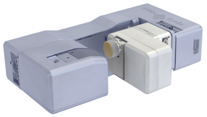
Image Credit: Oxford Instruments Materials Science
The integration of an exchangeable sample stage with a piezoscanner and a FemtoTools 2-Axis Microforce Sensing Probe allows for the implementation of advanced methodologies, including nano-scratch and nano-wear testing, in addition to SPM imaging, by enabling the in-plane movement of the sample while concurrently applying a normal force.
Specifications
Source: Oxford Instruments Materials Science
|
Travel range |
Noise floor |
| Piezo-Scanner |
20 µm |
50 pm |
Rotation Stage
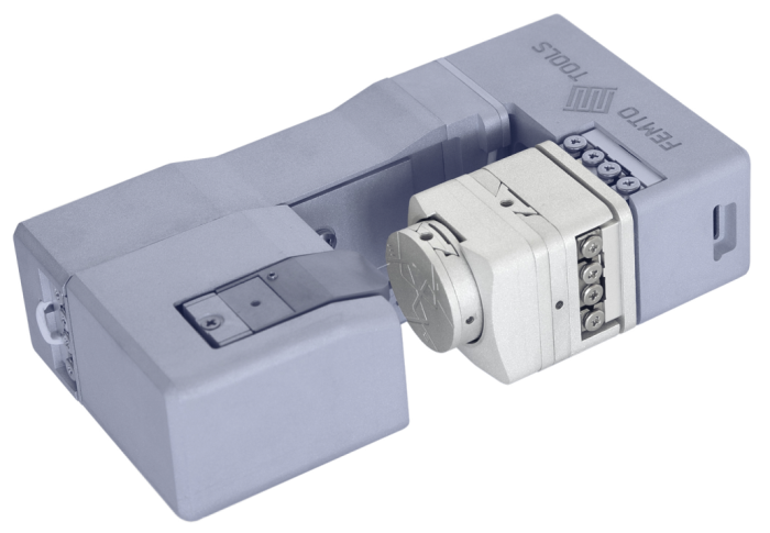
Image Credit: Oxford Instruments Materials Science
The rotation stage enables the rotary alignment of samples with the indenter tip, facilitating the testing of multiple samples in a single session by utilizing the rotation stage as a sample revolver. Furthermore, it enhances correlative nanomechanical testing by allowing for easy rotation of the sample between the indentation and imaging positions. Currently, it is not available in the USA and Japan.
Specifications
Source: Oxford Instruments Materials Science
|
Travel range |
Noise floor |
| Rotation Stage |
360 ° |
35 µ° |
Nano-Tensile Testing Chip
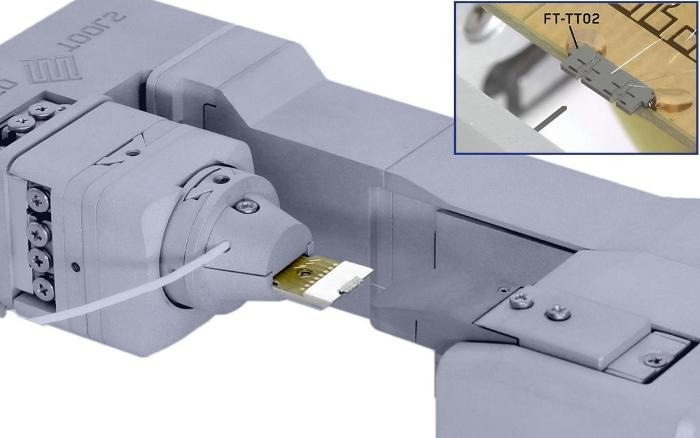
Image Credit: Oxford Instruments Materials Science
This MEMS-based Tensile Testing Chip features a movable body that is supported by four flexures within a stationary outer frame. It facilitates the tensile testing of samples that are thin enough to be electron-transparent, permitting concurrent imaging with Scanning Transmission Electron Microscopy (STEM) or Transmission Kikuchi Diffraction (TKD).
Specifications
Source: Oxford Instruments Materials Science
|
Gap sizes |
| Nano-Tensile Testing Chip |
100 µm |
50 µm |
10 µm |
7.5 µm |
5 µm |
Microforce Sensing Probes
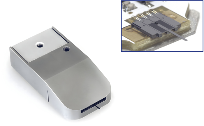
Image Credit: Oxford Instruments Materials Science
The FT-S Microforce Sensing Probes are advanced sensors designed to measure forces ranging from sub-nanonewton to two newtons along the axis of the sensor’s probe. The probes come in a diverse selection of tip materials and geometries, such as diamond Berkovich, cube corner, flat punch, wedge, conical, and others.
Specifications
Source: Oxford Instruments Materials Science
|
Force range |
Force resolution (noise at 10 Hz) |
| FT-S200 |
+/- 200 µN |
500 pN |
| FT-S2’000 |
+/- 2 mN |
5 nN |
| FT-S20’000 |
+/- 20 mN |
50 nN |
| FT-S200’000 |
+/- 200 mN |
500 nN |
| FT-S2’000’000 |
+/- 2 N |
5 µN |
Two-Axis Microforce Sensing Probe
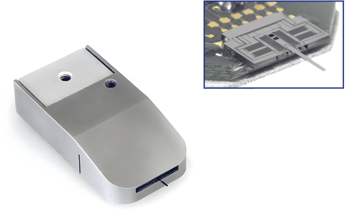
Image Credit: Oxford Instruments Materials Science
The FT-S Two-Axis Microforce Sensing Probes are multi-axis microforce sensors based on Micro-Electro Mechanical Systems (MEMS) that can measure forces simultaneously in two in-plane directions. These sensors are primarily utilized for applications such as nano-scratch testing, nano-tribology, and nano-wear testing.
Specifications
Source: Oxford Instruments Materials Science
|
Force range |
Force resolution (at 10 Hz) |
| Force Sensing |
+/- 20 mN |
100 nN |
| Tangential Force Sensing |
+/- 20 mN |
100 nN |
High-Temperature Microforce Sensing Probes
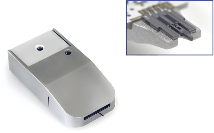
Image Credit: Oxford Instruments Materials Science
The High-Temperature Microforce Sensing Probes are microforce sensors based on Micro-Electro Mechanical Systems (MEMS) that can measure forces ranging from 200 mN to 2 µN. Additionally, the monolithically integrated tip heater allows for precise matching of the nanoindenter tip temperature to that of the sample, facilitating isothermal testing conditions.
Specifications
Source: Oxford Instruments Materials Science
|
Force range |
Force resolution (noise at 10 Hz) |
| Force Sensing |
+/- 200 mN |
1 µN |