The witec360 Semiconductor Edition is a high-end confocal Raman and photoluminescence (PL) microscope specifically configured for the chemical imaging of semiconducting materials. It helps researchers accelerate the characterisation of crystallinity, polymorphism, defects, strain, and doping in their semiconductor samples and wafers.
The microscope’s extended-range scanning stage enables the inspection of up to 12” (300 mm) wafers and the acquisition of large-area Raman images. It is equipped with vibration damping and active focus stabilisation to compensate for topographic variation during measurements over large areas or long acquisition times. All microscope components are fully automated, permitting remote-control and the implementation of standard measurement procedures.
Key Features
- Analysis of wide-bandgap semiconductors and layered structures
- Surface analyses, depth scans and 3D imaging
- Industry-leading confocal Raman and PL microscope for high speed, sensitivity and resolution – simultaneously
- Scientific-grade, wavelength-optimised Hexalight spectrometer for high signal sensitivity and spectral resolution
- Large-area scanning (300 x 350 mm) for wafer inspection
- Active focus stabilization for large-area measurements (TrueSurface)
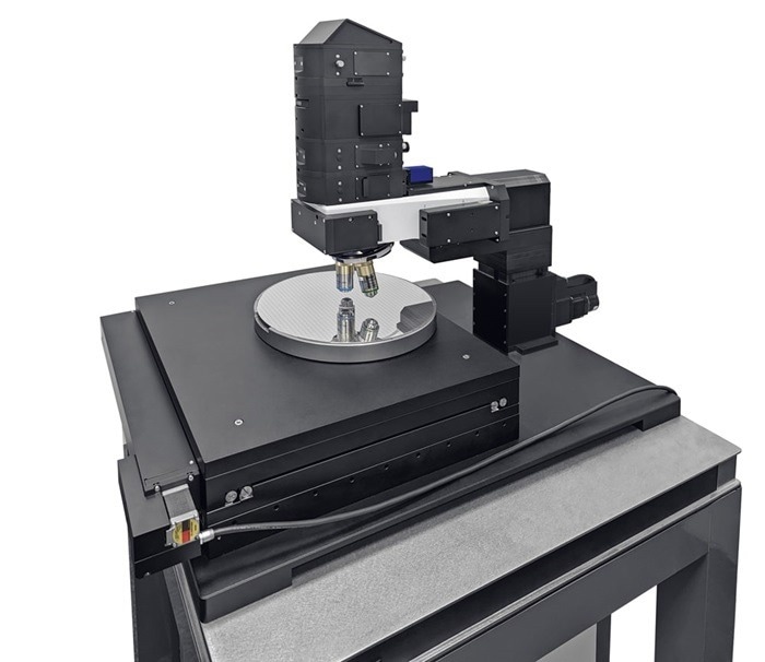
Image Credit: Oxford Instruments
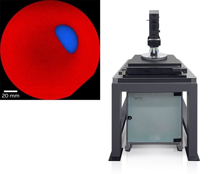
Image Credit: Oxford Instruments
Large-Area Wafer Inspection
For the semiconductor industry, ensuring wafer quality is of utmost importance. To assess the uniformity of the material and identify regions of strain or inconsistent doping, it is essential to thoroughly examine the entire surface area of a wafer.
In the example below, the complete surface of a 150 mm (6 inch) silicon carbide (SiC) wafer was imaged with Raman microscopy using a 532 nm laser for excitation. The analysis revealed non-uniform doping concentration across the entire area. The Oxford Instruments spectrometer detected peak shifts below 0.01 cm-1, exposing stress fields within the wafer.
To maintain a sharp Raman image of the entire wafer, it was crucial to actively keep the surface in focus. TrueSurface recorded the wafer’s topography and the Raman data simultaneously and compensated for height variations.
Furthermore, a depth scan through an epitaxially overgrown SiC wafer was recorded to visualize the distribution of the different layers. The sample was provided by the Fraunhofer Institute for Integrated Systems and Device Technology IISB in Erlangen, Germany.
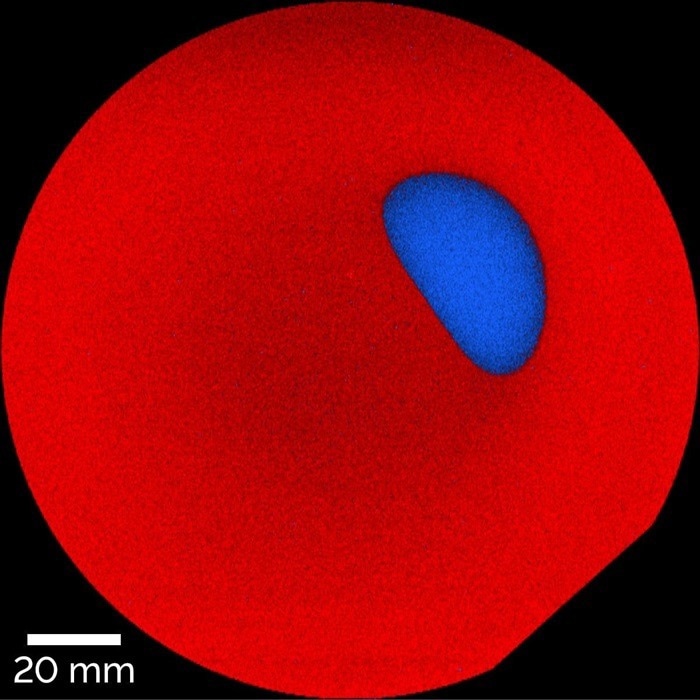
Confocal Raman image of a 150 mm SiC wafer. TrueComponent Analysis identified two spectra, which mainly differed in the doping-sensitive A1 peak (ca. 990 cm-1). The image reveals an oval region (blue) with a different doping concentration than the bulk wafer area (red). Image Credit: Oxford Instruments
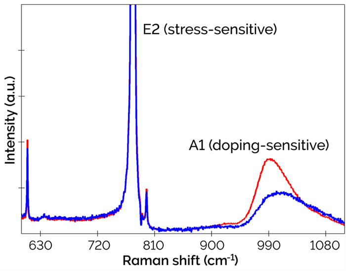
Raman spectra of the two components identified in the 150 mm SiC wafer by TrueComponent Analysis. Image Credit: Oxford Instruments
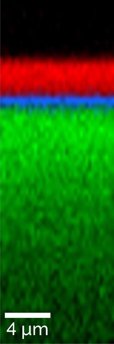
Raman depth scan of an epitaxially overgrown SiC wafer, showing a thin interface layer (blue) between the wafer substrate (green) and epitaxial layer (red). Image Credit: Oxford Instruments
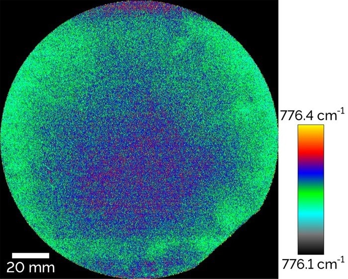
Confocal Raman image of a 150 mm SiC wafer, color coded for the position of the stress-sensitive E2 peak (776 cm-1). The image reveals a small, presumably stress-induced peak shift from the wafer’s center toward its edge. Image Credit: Oxford Instruments
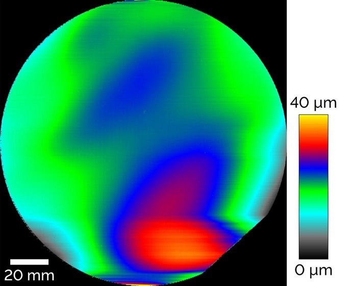
Topography of a 150 mm SiC wafer with height variations of up to 40 µm. Image Credit: Oxford Instruments
Specifications
- 300 x 350 mm scanning stage
- Active vibration damping
- DCOM interface for design and control of individual measurement procedures with LabVIEW, Python, C# and other programming tools
- Fully automated microscope control with AutoBeam Technology
- Highly sensitive, on-axis, lens-based, excitation wavelength-optimised spectrometer featuring thermoelectrically-cooled, scientific-grade spectroscopic CCD camera
- TrueSurface for active focus stabilisation and topographic Raman imaging
- Wafer chuck, optionally with vacuum pump
- White-light illumination for sample overview
- Workflow manager for streamlining recurring experimental tasks
- Various laser wavelengths are available
Benefits of Raman Imaging in Semiconductor Research
Confocal Raman imaging is a highly effective technique for both research and quality control within the semiconductor industry.
This technique can nondestructively acquire detailed, spatially-resolved chemical information about conventional materials such as silicon (Si), silicon carbide (SiC), gallium nitride (GaN), and gallium arsenide (GaAs).
It is also capable of investigating novel 2D materials such as graphene, perovskite, molybdenum disulfide (MoS2), tungsten diselenide (WSe2) and other transition metal dichalcogenides (TMDs) and heterostructures.
Raman images play a crucial role in visualising the spatial distributions of different materials, as well as material properties such as crystallinity, strain, stress, or doping. Depth scans enable the investigation of material distribution on substrates and characterization of interface layers, while 3D Raman images provide a means to depict inclusions within a sample.