Atomic force microscopy (AFM) is moving beyond surface imaging to reveal how materials behave, interact, and evolve at the nanoscale. This eBook explores advanced AFM modes that connect topography with mechanical, electrical, chemical, and optical insights, from quantifying adhesion and elasticity to resolving atomic lattices and moiré patterns in two-dimensional materials. It also examines how machine learning is helping researchers reconcile simulated and experimental results, identify regions of interest, and guide autonomous workflows. Throughout, the eBook underscores the importance of careful probe selection, calibration, and researcher oversight in turning high-resolution images into reliable quantitative measurements.
Download your free eBook
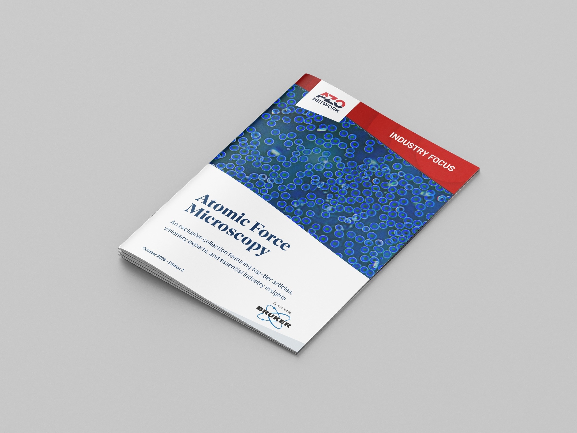
The eBook also explores emerging capabilities in two-dimensional materials, near-field optics, and intelligent microscopy. Readers will discover how AFM can resolve atomic lattices and moiré patterns, probe light confined to extremely small volumes, and use machine learning to help reconcile simulated and experimental results. The eBook also examines autonomous workflows that are beginning to guide microscopes toward regions of interest and suggest where to scan next, while keeping researchers firmly in control of the underlying scientific questions.
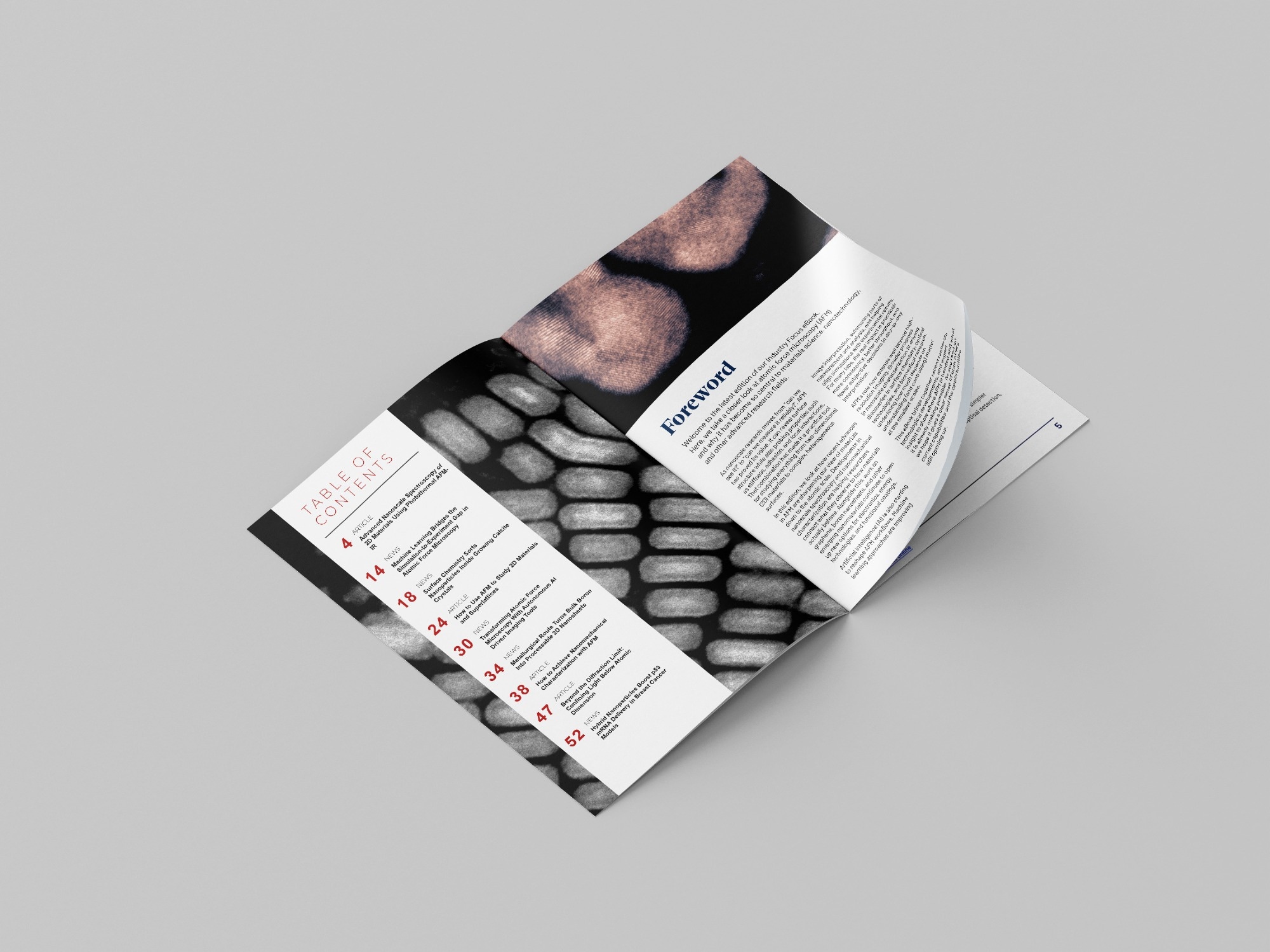
Drawing on examples from materials science, nanomanufacturing, and biomedicine, the eBook highlights how these advances are already supporting cutting-edge research. It explores how AFM is helping researchers understand the influence of surface chemistry on nanoparticle incorporation during crystal growth, evaluate the structure of processable boron nanosheets, and more. Together, these examples illustrate AFM's evolution into a more integrated analytical platform, providing a deeper look into nanoscale structure, chemistry, and function.
Download the full eBook here

Some of this information has been sourced, reviewed and adapted from materials provided by Bruker Nano Surfaces and Metrology.
For more information on this source, please visit Bruker Nano Surfaces and Metrology.