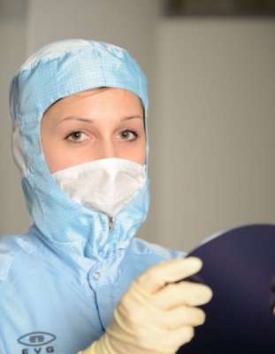
EV Group (EVG), a leading supplier of wafer bonding and lithography equipment for the MEMS, nanotechnology and semiconductor markets, today announced that it is developing equipment and process technology to enable covalent bonds at room temperature.
 EV Group announces ComBond(R) technology development for room temperature covalent wafer bonding. (PRNewsFoto/EV Group (EVG))
This breakthrough technology will be available on a new equipment platform, called EVG580® ComBond®, which will include process modules that are designed to perform surface preparation processes on both semiconductor materials and metals. EVG built on its decades of experience with plasma activated wafer bonding to create a novel process through which the treated surfaces form strong bonds at room temperature instantaneously without the need for annealing.
"In response to market needs for more sophisticated integration processes for combining materials with different coefficients of thermal expansion, we have developed a revolutionary process technology that enables the formation of bond interfaces between heterogeneous materials at room temperature," stated Markus Wimplinger, corporate technology development and IP director for EV Group. "Our unparalleled expertise in wafer bonding process technology will allow us to provide different variants of the new process according to the requirements of different substrate materials and applications."
EV Group's new process solutions will enable covalent combinations of compound semiconductors, other engineered substrates and heterogeneous materials integration for applications such as silicon photonics, high mobility transistors, high-performance/low-power logic devices and novel RF devices. The process technology and equipment that enables this room temperature covalent wafer bonding will be applied to EVG's wafer bonding solutions for MEMS wafer-level packaging as well as to the integration of MEMS and CMOS devices.
Equipment systems based on a 200-mm modular platform, tailored for the specific needs of the new processes, will be available in 2013.