EV Group (EVG), a leading supplier of wafer bonding and lithography equipment for the MEMS, nanotechnology and semiconductor markets, today unveiled the GEMINI®FB XT—its next-generation fusion wafer bonding platform, which combines several performance breakthroughs to move the semiconductor industry closer to the goal of high-volume manufacturing (HVM) of 3D-ICs with through-silicon vias (TSVs).
Featuring up to a three-fold improvement in wafer-to-wafer bond alignment accuracy as well as a 50 percent increase in throughput over the previous industry benchmark platform, the GEMINI FB XT clears several key hurdles to the industry's adoption of 3D-IC/TSV technology in order to drive continuous improvements in device density and performance without the need for increasingly costly and complex lithography processing.
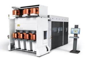 EVG(r)GEMINI FB XT Automated Production Fusion Bonding System for 3D-IC/TSV Manufacturing (PRNewsFoto/EV Group)
Wafer-to-wafer bonding is an essential process step to enable 3D devices such as stacked DRAM, memory-on-logic and future CMOS image sensors. At the same time, minimizing the dimensions of TSVs, which serve as the electrical contacts between the bonded wafers, is a key requirement for bringing down the cost of 3D devices and supporting higher levels of device performance and bandwidth, as well as lower power consumption. However, tight alignment and overlay accuracy between the wafers is required to achieve good electrical contact between the interconnected devices on the bonded wafers, as well as to minimize the interconnect area at the bond interface so that more space can be made available on the wafer for producing devices.
Alignment is key for fusion-bonded 3D-ICs
According to the 2012 edition of the International Technology Roadmap for Semiconductors (ITRS), high-density TSV applications will require wafer bonding alignment accuracy of 500 nm (3 sigma) by 2015. To enable high process yields for hybrid bonding, even tighter specifications are needed. The GEMINI FB XT incorporates EVG's newly introduced SmartView® NT2 bond aligner, which enables dramatically improved wafer-to-wafer alignment accuracy to below 200 nm (3 sigma). This corresponds to up to a three-fold improvement over EVG's widely adopted SmartView NT platform—the previous industry benchmark for bond aligners—and exceeds the latest ITRS Roadmap requirements, thereby filling a critical gap faced by device manufacturers that are considering adopting 3D-IC/TSV designs as part of their product roadmaps. An integrated metrology module validates alignment after pre-bonding to enable customers to quickly fine-tune the bonding process for HVM processing if necessary.
Leveraging EVG's XT Frame platform, which is utilized across the spectrum of the company's industry-leading systems, the GEMINI FB XT is optimized for ultra-high throughput and productivity. Additional pre- and post-processing modules have been added for wafer cleaning and surface preparation, plasma activation and wafer bond alignment that enable increases in throughput by up to 50 percent. This significantly increased throughput combined with the tighter alignment specifications supports IC manufacturers' efforts to move wafer stacking upstream in the manufacturing value chain from mid-end-of-line (MEOL) and back-end-of-line (BEOL) processing to front-end-of-line (FEOL) processing. This, in turn, enables device manufacturers to integrate more functionality into their product at the wafer level, where higher levels of parallel processing can significantly drive down 3D-IC/TSV manufacturing costs.
"While EUV lithography continues to face delays, 3D-IC/TSV integration has emerged as one of the most promising approaches to extending Moore's Law for future device generations. Yet enabling 3D-IC/TSV integration for emerging memory and logic applications is impossible without the ability to achieve tight wafer-to-wafer alignment," stated Paul Lindner, executive technology director at EV Group. "EVG is continuing to drive improvements across our suite of solutions for 3D-IC/TSV applications to help bring our customers closer to the goal of commercializing 3D-IC technology. Our new GEMINI FB XT platform marks a major milestone along that path, and we look forward to working with our customers to make the promise of 3D-IC high-volume manufacturing a reality for them."