This article describes some applications of fluorescence instruments from HORIBA to nanophotonics, e.g., singlewalled carbon nanotubes (SWNTs), quantum dots, and organic light-emitting diodes (OLEDs).
Quantum confinement affects nanomaterials’ photoluminescence: when the semiconducting nanoparticle is smaller than the bulk material’s Bohr-exciton radius, the bandgap energy is inversely proportional to the nanoparticle size. Smaller nanoparticles usually have higher energy absorbance and emission properties than larger nanoparticles of the same material.
SWNT Photoluminescence and the NanoLog®
Fig. 1 sketches the process of semiconducting SWNT photoluminescence. The decreasing absorption and emission energies of individual SWNT species correlate directly with diameters from analysis of radial breathing modes from Raman spectroscopy. Certain (n,m) values of semiconducting SWNTs match predicted bandgaps between valence and conductance bands. (Metallic and semi-metallic SWNTs with continuous valence- and conductance-bands show little or no photoluminescence.)
A NanoLog® (double-grating excitation monochromator, imaging emission spectrograph with a selectable-grating turret, and multichannel liquid-N2-cooled InGaAs-array detector) has optimal excitation optics for SWNT research or any solid sample in right-angle or front-face mirror configurations. The emission spectrometer has selectable gratings in a turret mount for rapid, easy acquisition of near-IR spectra. One grating has single-shot coverage of > 500 nm with a detector sensitive from 800–1700 nm.
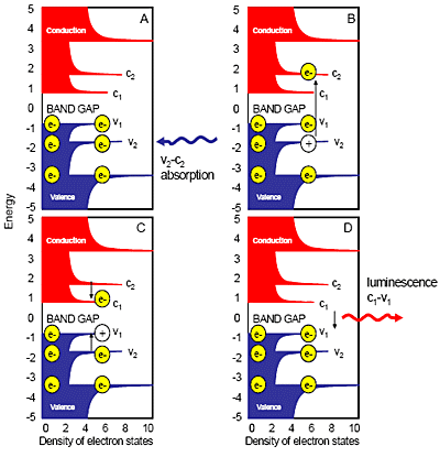
Figure 1. Semiconducting-SWNT photoluminescence absorption and emission. Conduction bands are red; valence bands are blue. Electrons are yellow; holes are white circles. Small black arrows are radiative or nonradiative transitions of e–s or holes between different band-levels. Vx and cx are specific valence or conductance bands.
Corrected emission spectra provide EEMs for a range of excitation wavelengths; acquisitions take only minutes. Excitation bandpass ranges from 0–14 nm; spectrometer slits vary from 0–16 mm with a 1200 groove/mm grating. An order-sorting filter prevents visible light from entering the spectrometer.
EEMs are compiled (Figs. 2A and B) by our exclusive NANOSIZER® software to determine SWNT composition (Fig. 2C). A double convolution algorithm (U.S. Pat. Pending) in the NANOSIZER® simultaneously computes excitation and emission wavelength coordinate line shapes for each species; contributions from all spectral bands in a region of interest are found. EEM data (Fig. 2, solid lines) and simulations (contour maps) from two SWNT suspensions of different manufacturing processes distinguished by different size and helical distributions are given: high-pressure carbon-monoxide method (HiPCO, Fig. 2A); cobalt-molybdenum catalytic method (CoMoCAT, 2B). Fig. 2A identifies five main HiPCO species; Fig. 2B indentifies four main CoMoCAT species. Fig. 2C, a helical map of species found in Figs. 2A and B, plots helical angle versus SWNT diameter against intensity of emission (symbol size). Note that HiPCO tubes have a larger mean diameter than CoMoCAT. The simulation gives precise analysis of SWNT composition on an IBM-compatible PC in minutes.
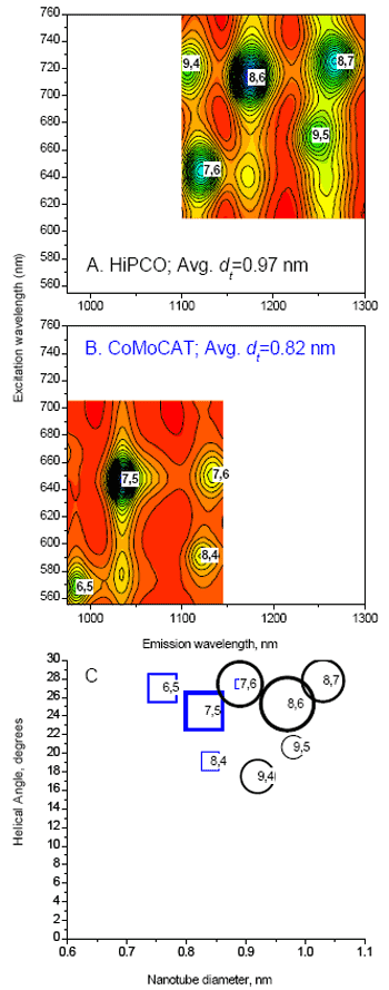
Figure 2. Quantum excitation-emission (A and B) and helical (C) maps of HiPCO and Co-MoCAT SWNT suspensions, using a NanoLog®. Solid lines (A and B) are data; color contours are simulations. Symbol sizes (C) show relative amplitudes for HiPCO (circles) and CoMOCAT (squares), each normalized to 1. R2 values for the simulations are 0.997 (HiPCO) and 0.999 (CoMoCAT).
Photoluminescence of Quantum Dots
Quantum dots’ absorption bands have broad spectral features and precise tunability of their emission bands. Their absorption spectra stem from many overlapping bands increasing at higher energies. Each absorption band corresponds to an energy-transition between discrete electron-hole (exciton) energy-levels; smaller dots give a first exciton peak at shorter wavelengths.
A photon is emitted when an electron crosses from conduction-band edge to valence band. Photon energy is proportional to bandgap, determined by the bulk material’s Bohr-exciton radius and the quantum dot’s size (Fig. 3).
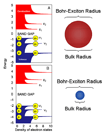
Figure 3. Quantum confinement for quantum dots. Valence and conductance bands are blue and red, respectively. Composition of dots A and B is identical; only the bulk radius varies relative to the fixed Bohr-exciton radius.
Quantum dots’ advantages compared to standard organic fluorophores are: A single source can excite multiple dots emitting over a broad range, giving selective exclusion of excitation light from the measured emission. Quantum dots have high fluorescent and strong two- photon absorption yields, so they are up to 1000 times brighter, for better imaging resolution. Their tunable bandgaps offer applications such as white-light LEDs and other displays.
Most quantum dots are made of toxic elements (e.g., Pb, Cd, Se, and Te). Their photoluminescence may be sensitive to biological interactions, so most biological applications of quantum dots require a coating (usually a triblock copolymer), rendering the dots non-toxic but also helping to conjugate the dots to molecular probes, and protecting the dots from biomolecular agents. Antibody conjugate imaging of these dots may be useful for diagnosis and treatment of cancer. Near-IR quantum dots may aid deeper tissue-imaging, for near-IR light penetrates tissue deeper than visible light. Quantum dots’ excited state lifetimes (2~10 ns) increase their worth for time-resolved fluorescence instruments. Many conjugation choices and excited-state properties of dots make them useful for biosensors based on fluorescence resonance energy-transfer.
Photoluminescent Analysis of OLEDs
Based on thin-films, OLEDs offer advantages over LCDs: no backlighting, emission of light only from active pixels for lower power, higher contrast and color-fidelity, brighter emission, wider viewing-angles, faster temporal response, better temperature-stability, and deposition on flexible or transparent substrates.
A voltage applied across an OLED circuit drives the electrons (Fig. 4A) and holes (Fig. 4B) into the organic layer where recombination occurs to emit photons (Fig. 4C). Here, photons from blue, green, and red emitters yield white light. Composition, thickness, and relation between the various layers regulate OLED luminescence.
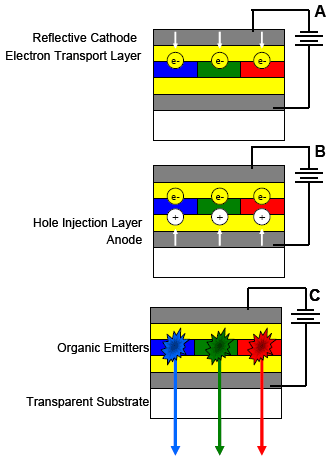
Figure 4. OLED operation in 3 stages, A to C. White arrows show flow of e–s (yellow) and holes (white) from electrodes. Starbursts in C are electron-hole recombination in the organic layer followed by photon emission.
Fig. 5 shows the phosphorescent decay of a Universal Display emitter with a lifetime of > 1 µs, recorded on a TCSPC-Fluorolog®.
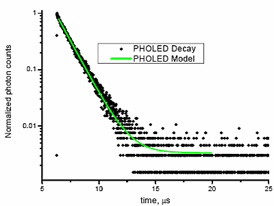
Figure 5. Phosphorescent decay of an organic emitter from a PHOLED, using a TCSPC-Fluorolog® in front-face mode (for solid samples), resolving from <100 ps to > 200 µs. ëexc = 335 nm NanoLED (800 ps pulses); ëem = 520 nm. R2 for the tail-fit = 0.995.
HORIBA Instruments for Quantum Dots and OLEDs
The modular Fluorolog® spectrofluorometer is equipped for UV to near-IR steady-state and time-resolved measurements (from <100 ps) for photoluminescence research. The instrument can do steady-state and time resolved anisotropy for molecular motions and shapes, with two TCSPC detectors: our TBX-05 (300–850 nm, 180 ps), and the Hamamatsu 9170-75 (900–1700 nm, 300 ps). Monochromators and gratings blazed for UV-visible or near-IR in the T-format can optimize the system. A switchable adapter for xenon lamp and NanoLED converts between steady-state and time-resolved modes. NanoLEDs are pulsed TCSPC light-sources (~1 ns to = 200 ps, 10 kHz–1 MHz repetition rates), including deep-UV (265, 280, and 295 nm), and are interchangeable with SpectraLEDs (500 ns pulses to CW) for phosphorescence studies.
Cell-imaging, biosensing, and nanophotonic circuit-analysis require microscopic resolution, broad spectral sensitivity, and wide dynamic and kinetic ranges, provided by our modular DYNAMIC™ confocal microscope with steady-state ps-to-ns time resolution, and mapping to 1 µm.
The system can be coupled to the Fluorolog®. Fig. 6 shows CdS quantum dots in a semiconductor wafer, along with the dots’ spec- tral contribution (ëexc = 350 nm).
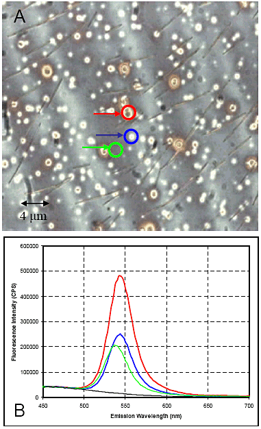
Figure 6. Spectral and spatial mapping of CdSe quantum dots in a solid state matrix of a semiconductor wafer. A is the bright-field image; color-coded spots for spectral regions of interest are emission spectra (B).
Conclusions
For researchers of SWNTs, we offer the NanoLog® and NANOSIZER®. Researchers of quantum dots can use our Fluorolog®. For maturing OLED technology, we have TCSPC instruments to resolve fluorescent lifetimes. Biological applications will find the DYNAMIC ™ important. HORIBA has the optimum spectrofluorometer for nanotechnology research in these areas.

This information has been sourced, reviewed and adapted from materials provided by HORIBA.
For more information on this source, please visit HORIBA.