High-brightness light emitting diodes (HB-LEDs) are mostly formed on sapphire wafers. Patterning the substrates with tiny structures ensures a drastic improvement in the light extraction efficiency of the completed device. PSS wafers also solve critical issues that include crystal dislocations and refractive index mismatch.
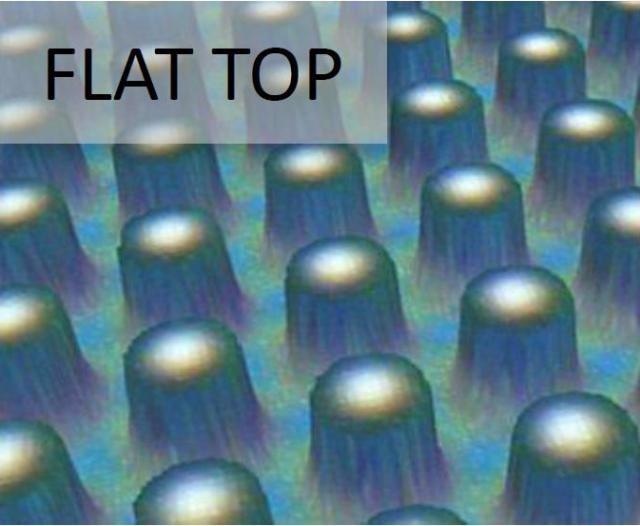
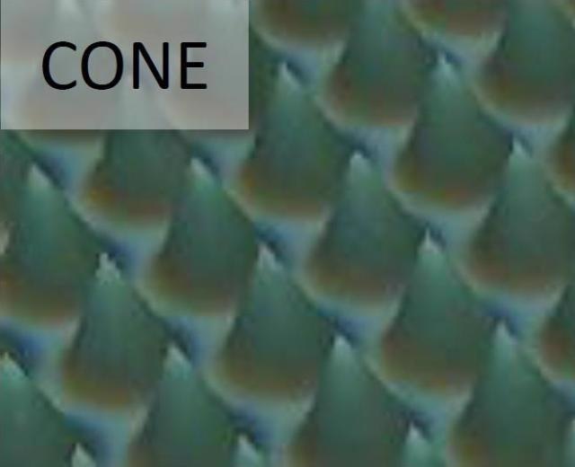
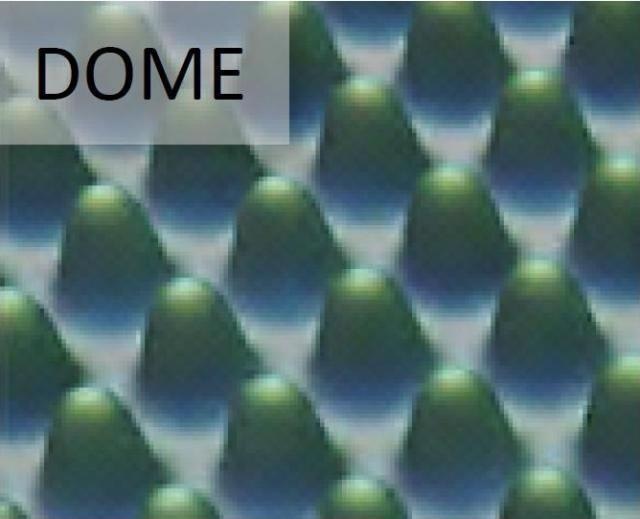
The Zeta-PSS Package offers quick characterization of substrate bump features. Height, width, and pitch are determined in the same scan. Recipes are available for all types of substrate bumps that include cone-shaped, dome-shaped, flat-topped, or photoresist.
Zeta Optical Profile System
The Zeta Optical Profiler System includes the following salient features:
- Automated feature analysis
- Exceptional measurement potential
Automated Feature Analysis
This feature is easy to use and production-ready and is capable of the following:
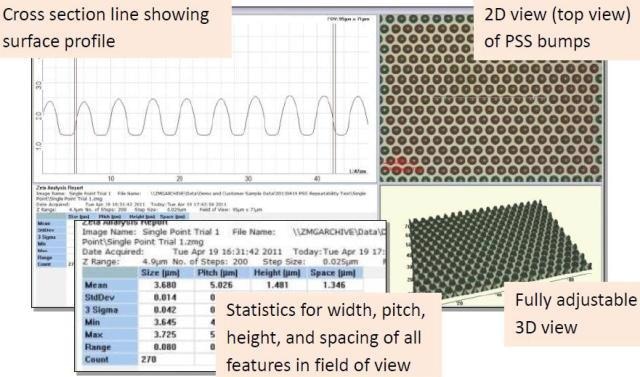
- The Zeta Optical Profiler takes a large area scan (70 µm x 90 µm) in seconds.
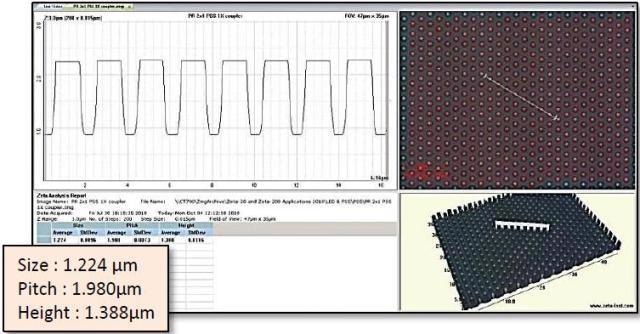
- Using the Zeta 3D software, a one-page analysis report can be obtained that includes 2D and 3D images, a cross section, and statistical analysis of all features in the field of view.
- Numerical results are saved in spreadsheet-friendly text format.
- Automated X-Y stage and multisite recipes allow characterization of the entire wafer.
Exceptional Measurement Capability
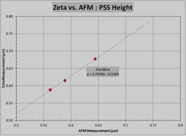
Zeta Optical Profiler measurements of height and width correlate well with those obtained with the AFM.
Optional Piezo Z stage provides 2nm Z-height resolution and 3s repeatability below ±15nm
The specific features and options of the Zeta-PSS Package include the following:
- Manual load system for R&D and automated XY stage for production
- Vacuum chucks for wafers of different sizes
- Vibration and Environmental noise isolation package Piezo stage for 2nm height resolution
- True color 3D imaging enable review of defects such as scratches or missing bumps
Zeta 3D Software analyzes standard 2D or 3D wafer images for general surface characterization:
- Step height
- Surface roughness
- Feature size, diameter, area, and volume
- Wafer bow
- 3D surface visualization in true color
- Statistics
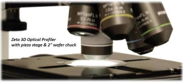
Zeta 3D Optical Profiler with piezo stage & 2” wafer chuck
Customized PSS analysis software includes production-ready recipes for cone, dome, and flat-topped bumps. Hardware includes Zeta’s unique PSS specific illumination optics.

This information has been sourced, reviewed and adapted from materials provided by KLA Corporation.
For more information on this source, please visit KLA Corporation.