EVG offers a wide range of equipment and processing solutions for their microfluidics customer base regardless of where they are at in the product life cycle. Whether you are in early stage R&D or looking to move your product into high volume manufacturing, EVG provides dedicated equipment for microfluidics manufacturing. Whether it means assisting its customers with their prototyping needs or customizing the right automated tool for a specific set of processing constraints, EVG will work closely to assure the highest quality of service.
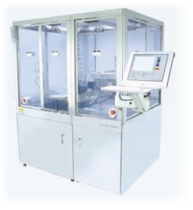
Figure 1. The EVG®750 - the world´s first and only fully-automated hot embossing system for microfluidic device fabrication.
Equipment
At EVG, all standard equipment offerings come in versions that allow its customers to move smoothly up the value chain, from R&D to High Volume Manufacturing. Thus EVG have a complete array of processing equipment for its microfluidic customer requirements.
The list of EVG equipment sets for microfluidic fabrication are:
- Resist Processing Systems
For over 30 years, EVG has been a mainstay in the lithographic market with focus on MEMS devices. Thus, for customers with non-polymeric substrate needs EVG offer a range of products for cleaning, coating, exposure and develop.
- Hot Embossing
EVG offers the widest range of hot-embossing systems - including the only automated hot embossing systems on the planet:
EVG 510HE: Semi-Automated R&D Solution
EVG 520HE: A solution to take you from R&D through to pilot production.
EVG750: The world's first automated Hot Embossing system - automates the entire process flow for throughputs above 10 substrates per hour.
EVG GEMINI: The world's first automated cluster tool available in a dedicated configuration for microfluidic fabrication. The system leverages its decades of experience in automated production wafer bonding systems. This highly configurable system provides maximum flexibility for microfluidic fabrication with process such as: cleaning, coating, hot embossing, plasma activation, aligned bonding and allows for OEM, customer specific, modules to be added-on. Talk to us today about how EVG can customize a GEMINI system for your specific manufacturing needs.
- Bonding
All of the hot embossing systems above can be configured for bonding - both aligned and unaligned. The hot embossing systems can also serve a dual role (hot embossing and bonding) with simple tooling changes.
- Plasma Activation
The EVG810LT system provides bonding of polymer substrates below their glass transition temperatures.
- Cleaning
The EVG300 Series of systems and modules allow microfluidic customers to apply DI water and dilute chemistries with a megasonic head for a variety of cleaning applications.
Working Stamp Processing
EVG's working stamp technology allows for rapid and cost-effective prototyping of microfluidic piece parts. EVG stamp material can emboss into thermoplastic materials below ~ 150°C. The working stamp fabrication process is accomplished on-site in a UV exposure process and can use any virtually any known hard stamp for replication (e.g. metals, silicon, glass, resists, etc.). The material has inherently low surface energy, thus no anti-stiction coating is necessary. Feature size resolution has been proven from the macro-scale (~ millimeters) down to the extremely small (~ 50 nanometers) with excellent fidelity from the hard master.
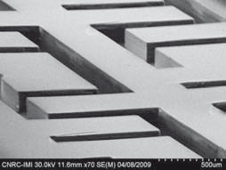
Figure 2. SEM Image of 200 μm hot embossed micro fluidic channels. Source: IMI-CNRC
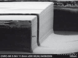
Figure 3. SEM Image of 20 μm hot embossed micro fluidic channels utilizing polymeric stamps (height 180 μm). Source: IMI-CNRC.
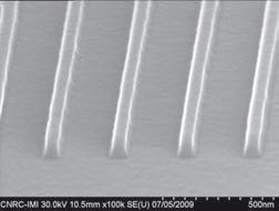
Figure 4. SEM Image of 50 nm hot embossed liness utilizing polymeric stamps. Source: EVG.
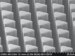
Figure 5. Super dense, high aspect ratio (30 μm tall; 9 μm wide) separation columns embossed on the EVG750 with working stamps. Source: IMI-CNRC
Process Services and Development
EVG, along with a core group of prototyping partners, can assist you in developing prototypes from design through to patterned and capped parts. At its applications labs in Europe (Schaerding, Austria), North America (Tempe, AZ) and Japan (Yokohama), EVG offers a wide array of process services to its microfluidic customers. These labs are class 100 or better providing excellent cleanliness. These facilities can also provide limited pilot production capability.
Supported process services and development work include:
- Resist Processing
For customers that are using traditional substrates like glass and silicon EVG can process your devices from design to resist patterning.
- Hot Embossing
EVG systems can emboss into all thermoplastic polymers and EVG can also use its proprietary polymeric working stamp technology (see below) to rapidly prototype your parts while maintaining the integrity of your hard stamp. EVG can also emboss into certain glasses with glass transition temperatures below ~ 630 °C.
- Plasma Activation
EVG's plasma activation can be used to activate the surface of thermoplastic polymers allowing them to bond to themselves and other materials at temperatures EVGll below their glass transition temperature. This allows for strong thermal compression bonding while preserving your embossed structures and/or any biologics that have been functionalized on the polymer surface.
- Bonding
EVG offers a wide range of bonding processes from thermal compression to adhesive to anodic. Tell us about your bonding needs and EVG will design the right solution for your device.
- Alignment
EVG can provide alignment for hot embossing and bonding requirements. Specifications depend on your particular process and material but EVG has equipment and process capability to bond with single-digit micron accuracy - in fact, deep sub-micron bonding alignment is possible with the right materials and processes!
- Cleaning
EVG has in-house capability to perform cleans with DI water and dilute chemistries - providing the capability to minimize defects and maximize yield - even on prototyping devices.
This information has been sourced, reviewed and adapted from materials provided by EV Group.
For more information on this source, please visit EV Group.