Moore's Law states that the density of transistors on a chip will increase exponentially - doubling in performance every two years. The computing industry has managed to adhere to this law since it was first proposed by Gordon Moore in 1965. However, this prediction only considers silicon-based CMOS (complementary metal-oxide semiconductor) technology.
This technology has limits which will must eventually break the exponential trend. This article explores some of the ways in which the lifetime of CMOS microprocessors can be extended, and some of the technologies which are being suggested as replacements.
Limits to CMOS Scaling
There are three main limits to the continued down-scaling of CMOS feature size:
- Capabilities of the fabrication method
- Decreasing switching performance
- Increasing leakage (spontaneous switching of states, leading to errors and data corruption)
There have been multiple points in the history of computing where CMOS technology has been predicted to hit a limit.
Engineers in the microchip industry have an excellent track record for getting around seemingly unbreakable performance limits. Because of this, CMOS technology and Moore's Law will probably continue for much longer than many commentators currently claim.
However, as quantum effects begin to have a much stronger effect on the behaviour of the electronic components in microprocessors, silicon will become unworkable, and new materials and designs must be employed to continue to meet the demand for increasing performance in microelectronics.
Michio Kaku: Tweaking Moore's Law and the Computers of the Post-Silicon Era | Big Think
Figure 1. Physicist Michio Kaku outlines the limitations of silicon-based computing, and explains his pick for the most likely successors to the technology.
Carbon Nanotubes and Graphene as Transistor Materials
A large part of the buzz surrounding nanostructured carbon materials like carbon nanotubes (CNTs) and graphene in the last few years has been centred on their potential for use as transistors.
These materials have unique electronic properties, because of the quantum effects of their dimensional restrictions. They have been shown to possess very useful qualities for use in nanoelectronics.
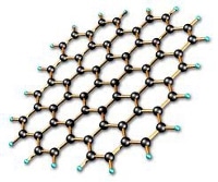 |
| Figure 2. Graphene could be the basis of the next generation of transistors. Image credit: LBL.gov |
| In February 2010, an article in Science was published reporting on joint work by IBM and DARPA which created a graphene processor with a 240nm gate length capable of a clock speed of 100GHz, around four times faster than any previous graphene-based transistors. Silicon-based processors with a similar scale of architecture only capable of around a 40GHz clock speed. |
However, the precise physical structure of the materials can lead to a large range of properties, particularly in CNTs. There are difficulties associated with manufacturing CNTs with a particular structure on a large scale, as most existing techniques tend to produce a mixture of forms.
Fabrication and separation processes are getting better all the time, however. Graphene is likely to start appearing in computing applications relatively soon.
Molecular Electronics
Molecular electronics aims to make components like transistors and logic gates from single molecules. Several potential candidates for molecular devices like these have been proposed.
However, a fully integrated chip using solely molecular components has not yet been achieved, and there are some serious manufacturing issues to overcome before the technology can be considered for commercial applications.
The benefits of molecular electronics would be extraordinary, however. The power consumption and data density which would become achievable once the initial design and manufacturing challenges have been overcome are incredible. Molecular electronics is potentially capable of providing a clear pathway to sub-nanometre chip architectures.
Photonics
Photonics uses photons, or particles of light, to conduct calculations, instead of electrons. This is an emerging field, which depends on highly advanced materials and fabrication techniques which are entirely different to the methods used with CMOS.
The expense of manufacturing exotic optical materials on a large scale will probably preclude optical computing from reaching mainstream markets any time soon. However, the huge computing speeds and low power consumption will probably drive adoption of photonic system for more specialized, large-installation supercomputing applications.
Ferromagnetic Devices
Ferromagnetic materials contain many distinct nanoscale regions, called domains, which can behave independently to some extent - the magnetic field of neighbouring domains can point in different directions.
There has been a considerable amount of research into using ferromagnetic materials as the basis for data storage and microprocessors - using the direction of magnetization of individual domains to represent bits of information.
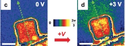 |
| Figure 3. Imaging of ferroelectric material shows their response to external current. Image credit: BNL.gov |
|
In July 2012, a research team at the U.S. Department of Energy's Brookhaven National Laboratory published a technique for studying exotic ferroelectric materials, revealing details on a sub-atomic level.
Ferroelectric materials work in a similar way to ferromagnetics, but with local electric field domains.
the published technique will help to develop applications for these materials in nanoelectronics.
|
The intrinsic properties of ferromagnetic materials makes data stored this way highly stable - the domains are non-volatile and resistant to radiation. Patterning of ferromagnetic wires can also produce effective logic gates.
Current Status of Research
Most of these technologies are still in their infancy. However, the huge pressure on the industry to continue to hold to Moore's Law means that the process of bringing a novel, esoteric technique to commercial fruition is often much more rapid than in other fields. This relentless drive is already resulting in the most advanced results on graphene-based electronics, molecular transistors, and ferromagnetic devices.
In the meantime, microprocessor manufacturers are stretching the capabilities of CMOS chips as far as they can. Intel's Ivy Bridge series, released in early 2012, features a 22nm architecture, achieved using a 3D "fin" design, and they plan to introduce 14nm processors in the 2013-2014 timeframe.
The long term picture will definitely feature the demise of CMOS technology, however. How much longer manufacturers can continue to uphold Moore's Law remains to be seen, but there is no doubt that microprocessors, and nanoprocessors, will continue to advance at a furious rate, no matter which technological pathway is chosen.
References