Structured substrates are extensively used in semiconductor research, more particularly in the development of semiconductors. There is a growing need to thoroughly understand the inherent strain and crystalline properties of device structures due to a high demand for device reliability and quality.
This article covers 3D confocal Raman imaging measurements that show signal changes, which can be attributed to strain and also to changes in the lattice structure.
Sample Description
The sample utilized was a doped GaN layer of 20µm thickness grown by metal organic vapor phase epitaxy (MOVPE) and subsequent overgrowth is done by hydride vapor phase epitaxy (HVPE) on a c-plane patterned sapphire substrate (PSS).
The Ferdinand-Braun Institute in Berlin performed fabrication and growth of the pattern. I-line beam stepper lithography was used to pattern the sapphire substrate with a KMPR 1000 negative photoresist and ion coupled plasma (ICP) etching. The honeycomb-like structure being studied has a ridge width of 3.5µm with a trench depth of 4.5µm and a pitch of 12µm.
This as well as similar patterns are relevant for LEDs as they enable epitaxial lateral overgrowth to bring down the threading dislocation density and enhance the internal quantum efficiency or serve for embedded periodic deflectors to improve light extraction.
Figure 1 shows a cross-sectional SEM micrograph of the sample.
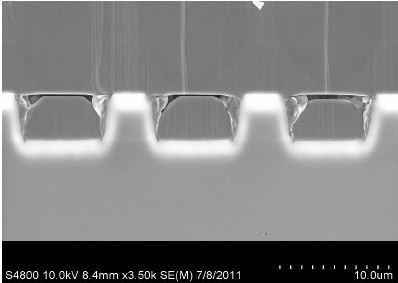
Figure 1. SEM Image of the structures - Vertical lines are steps due to cleavage with a higher line density in regions of direct contact between GaN and sapphire.
Figures 2a, b, and c contain SEM images of the pattern after the ICP process in 2(a), after the growth of the first 3µm thick GaN film on the PSS substrate by MOVPE as shown in 2(b), and after the growth of another 17µm thick GaN layer by HVPE as shown in 2(c).
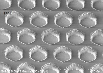
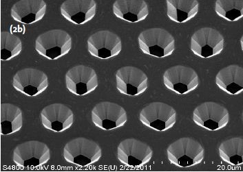
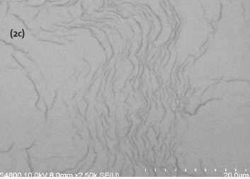
Figure 2. SEM Images of the structures after the etching process (a), after the growth of the first 3 pm GaN film (b), and after the growth of the additional 17 um thick GaN layer (c).
Experimental Framework
The experiment steps are as follows:
- An alpha300R+ confocal Raman microscope with a frequency-double Nd:YAG laser for excitation (1=532nm) was used to examine the sample.
- The light was coupled into the microscope using a single-mode fiber and brought onto the sample using a dichroic mirror and a 100x NA 0.9 air objective.
- In the detection beam path, the Rayleigh-scattered light was filtered out by means of an edge filter and a 50µm core-diameter fiber was utilized as a confocal pinhole, offering good depth resolution while maintaining superior collection efficiency. The light was then directed to a UHTS300 spectrometer fitted with an EMCCD camera and a 1800g/mm grating (BLZ 500nm).
- The sample's XY positioning was obtained using a piezoelectric scanning stage, and a stepper motor was utilized for the focus control (10nm single step).
- The Raman spectra were recorded as a depth scan along an interesting axis of the sample, as shown in Figures 3 and 4.
- 3D stack scans were further performed and examined (180x45x20 points with a scan volume of 60x15x20µm3).
- Using the WITec Project Plus data analysis software, the information relevant to the spectra was obtained and displayed as color-coded Raman images.
Results and Discussion
Figure 3 shows the white-light image of the sample obtained using the integrated ocular video camera and the stitching function of the system. The red square in the image denotes the area from which the high-resolution white light image was taken using the 100x objective (Figure 4). The green area in Figure 4 depicts the area at which the XY and the stack scan was carried out. The red line denotes the plane in which the single depth scan was carried out.
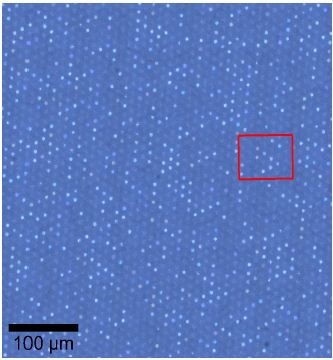
Figure 3. Stitched image of the sample acquired using an ioox objective. The red square shows the position of the high-resolution video image shown in figure 4.
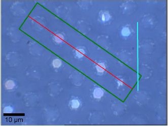
Figure 4. Video image of the area of interest. The area of the stack scans is shown in green and the red line shows the position of the single depth-scan.
Analysis of Spectral Features in Sample
It was possible to detect three areas in the sample using a depth-scan. Figure 5 illustrates the false-color Raman image with the spectra in corresponding colors displayed in Figure 6. In the areas with magenta color, the spectrum displays the typical features of GaN spectra, while an enhanced fluorescence can be seen in the green areas. This fluorescence is mainly located in the low wave number range of the spectrum.
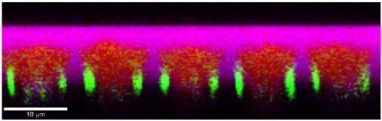
Figure 5. Color-coded Raman image of the depth scan performed along the red line shown in figure 4. The magenta, red and green areas correspond to the spectra shown in figure 6. The holes in the structure were located exactly underneath the red areas. The height of the structure appears to be reduced due to the difference in the refractive index between air (~i) and GaN (2.45).
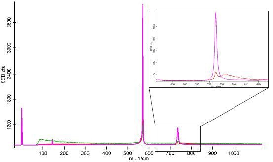
Figure 6. Color-coded Raman spectra corresponding to the Raman image shown in figure 5. In the zoomed view the green spectrum is omitted for clarity.
Figure 7 illustrates a layer obtained from the stack scan in which the typical spectral features are again shown utilizing the same color code. It can be seen that the fluorescence (green areas) is present at the walls of the ridges. The areas of lower intensity of the 735 rel.1/cm peak are present at the inner side of the holes.
The layers recorded in the image stack were studied similar to the layer illustrated in Figure 7 and integrated into a 3D reconstruction using the Image J software. A 3D view of the reconstructed 3D structure is shown in Figure 8.
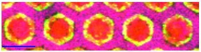
Figure 7. Color coded Raman image of a single plane extracted from the stack scan. The magenta, red and green domains correspond to the spectra shown in figure 6.
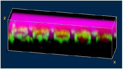
Figure 8. Color-coded 3D Raman Image of the structure. The colors correspond again to the colors of the spectra shown in figure 6.
Peak-shift Analysis
Using the above measurements, a peak-shift analysis of the spectra was carried out. For this purpose, the peak near 570 rel.i/cm of each spectrum in each of the scans was fitted using a Lorentzian curve. This helps in precise determination of the position of the Raman peaks with a typical uncertainty of 0.02 rel.i/cm.
Conclusion
3D confocal Raman imaging was utilized to study the characteristics of GaN layers grown on patterned sapphire substrates. It has been demonstrated that an improved fluorescence signal can be identified along the perimeter of the etched structures and that the material beyond this region displays a clearly modified Raman spectrum when compared to bulk GaN with an additional tensile strain component.

This information has been sourced, reviewed and adapted from materials provided by WITec GmbH.
For more information on this source, please visit WITec GmbH.