With the increasing trend towards miniaturization in microelectronic devices, a strong structural understanding of materials at the nanoscale is becoming a requirement for the fabrication of reliable products.
Nanoscale failure analysis usually requires a focused ion beam (FIB-SEM) along with nanomanipulation tools, to extract specific regions of interest. Structural and analytical characterization of these lift-outs is normally performed in a TEM. This is a complicated analysis procedure, and there are restrictions on the size of area which can be examined.
Alternatively, for these applications, the technique of electron backscatter diffraction (EBSD) can be applied either in FIB-SEM or FEG-SEM fitted with EBSD systems.
This article describes a method of combining Oxford Instrument's OmniProbe tools and AZtec EBSD system for the manipulation and analysis of a 5µm diameter gold microelectronic wire sample.
Gold Wires
Junctions on micro-electronic devices are often made using gold wires in a range of sizes. The grain size distribution and the crystallographic texture of the wires have an impact on the electrical and lifetime properties of the devices in which they are used. Therefore, it is very important to understand and control these parameters to enhance the performance and the reliability of these devices.
It is not possible to use traditional methods of polishing, sectioning and polishing due to the fine size of the gold wires. A solution is to use an OmniProbe nanomanipulator combined with FIB-SEM tools to select regions of interest, to lift them out, and then to position them correctly for EBSD analyses. For instance a 5 µm diameter gold wire is used to demonstrate this technique.
Experimental Procedure
The OmniProbe 100 and a FIB-SEM are used for cutting and transferring the sample to an SEM with an EBSD system. Figures 1 and 2 show the steps taken for cutting the wire and mounting and positioning for EBSD analyses. The steps are as follows:
- Attach 5µm gold wire onto carbon adhesive disc as shown in Figure 1a
- Navigate to region of interest and deposit platinum protective layer onto the wire as in Figure 1b
- Cut coated section using FIB as in Figure 1c and cut excess carbon adhesive disc from section as in Figure 1d
- Attach cut section to a lift-out OmniProbe needle as in Figure 2a and 2b
- The cut section is oriented and attached to a sample holder, in this case a standard TEM grid - Figure 2c and 2d
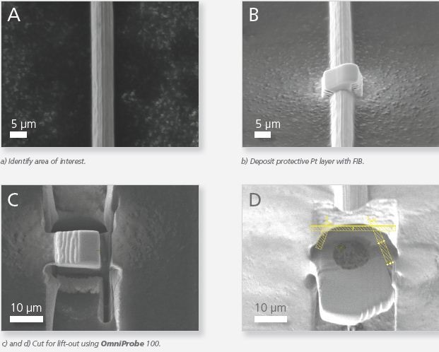
Figure 1. Ion images: steps of sample preparation using FIB and OmniProbe Tools.
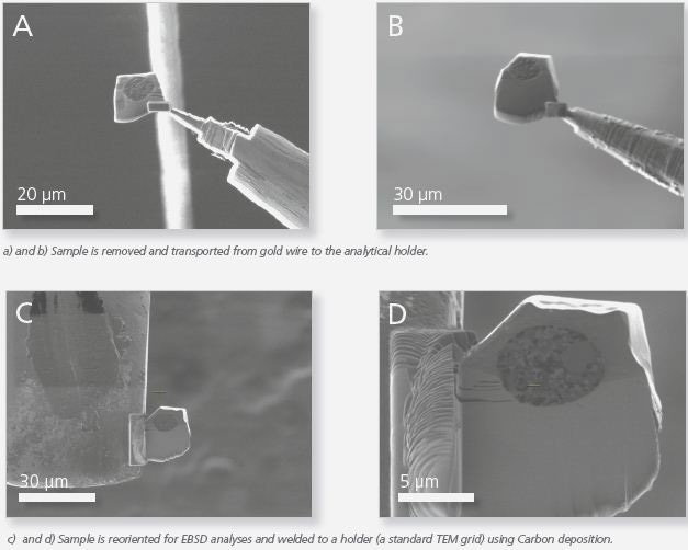
Figure 2. Attach and orientate section for analysis.
EBSD Analyses
The sample is positioned and attached to the TEM grid and then transferred to a FEG-SEM for EBSD analyses. The Oxford Instruments NordlysNano EBSD detector along with an AZtec system was used for characterizing the the microstructure of the sample.
Figure 3 shows a secondary electron image of the extracted gold wire section. In a FEG-SEM the sample was tilted at 70°. Using the parameters listed in Table 1, EBSD analysis was done.
Table 1. EBSD acquisition parameters details.
| Acceleration voltage |
Step size |
Camera binning mode |
Acquisition time |
Acquisition speed |
Hit rate |
| 15 kV |
15 nm |
8x8 |
45 min |
64.5 Hz |
92 % |
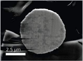
Figure 3. SE image of gold wire section tilted at 70° for EBSD analyses. The grain structure can be clearly seen.
Results and Discussion
IPF colored maps and EBSD band contrast are shown in Figure 4. a and b respectively. Figure 4b shows that the crystallographic direction of the grains are aligned along the axis of the gold wire.
The pole figures in Figure 6 show that the alignment is along the <111> and <001> directions and the wire has a dominant {111} fibre texture and a weaker {001} texture component. The fractions of the {111} and {100} components are 84% and 16% respectively. 16% is distributed mainly in the wire’s central region and a large grain to the top right of the section.
0.24µm is the average grain size in this section and a histogram of grain size distribution is shown in Figure 5. The comparatively course grain observed on the section’s right side has a {100} orientation, is over 1.8µm in diameter and dominates the cube component in pole figures in Figure 6.
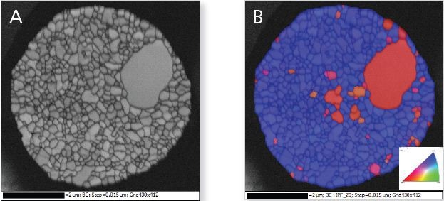
Figure 4. a) EBSD band contrast image. b) IPF (Z direction) of the long axis of gold wire.
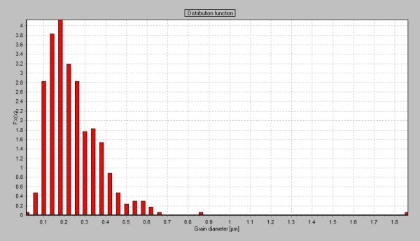
Figure 5. Histogram of grain size distribution - average grain size in this section is 0.24 jm.
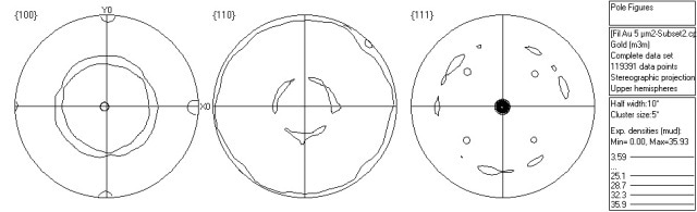
Figure 6. Set of {100}, {110} and {111} pole figures from analysed gold wire sample.
Figure 7 shows a set of ODF sections at φ2 (Euler3), showing a dominated {111} fiber texture of the gold wire and a cube {100} texture from the coarse grain.
For quantifying the preferred orientation tendency f(g), Figure 8 shows the orientation density across the cube {100} and {111} components (for φ1 and φ2 = 45°) as a function of f. The maximum intensities found in the ODF are {111} and {100}.
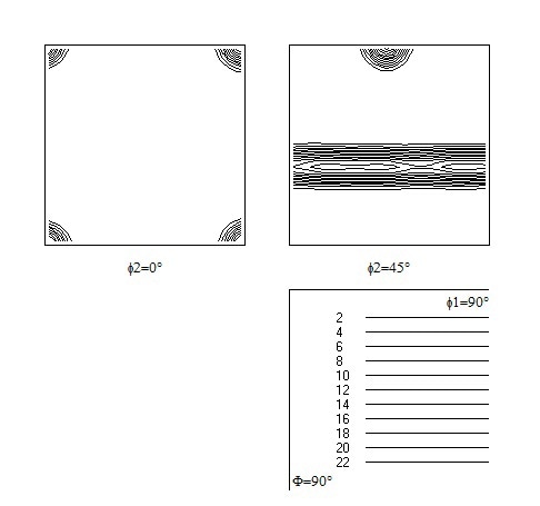
Figure 7. ODF sections at φ2 showing the strong {111} fiber texture of the gold wire and a cube {100} texture from the coarse grain.
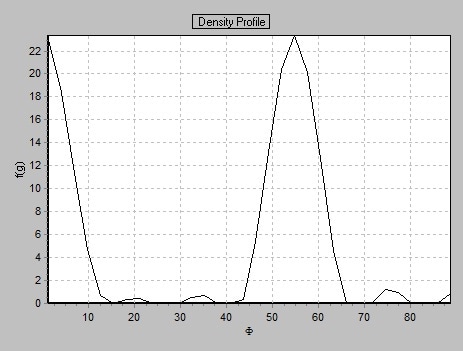
Figure 8. Orientation density f(g) of gold wire across the cube {100} and {111} components for φ1 and φ2 = 45°.
Conclusion
The analytical approach presented in this article describes the accurate and straightforward way to prepare, manipulate and analyze very localised sample regions.

This information has been sourced, reviewed and adapted from materials provided by Oxford Instruments Nanoanalysis.
For more information on this source, please visit Oxford Instruments Nanoanalysis.