Carl Zeiss, a leading global provider of electron- and ion-beam imaging and analysis solutions, today presents its newly developed line of corrected LIBRA 200 transmission electron microscopes (TEM).
 Aberration free high resolution imaging of a YAG crystal interface at 200 kV. [Courtesy of Katharina Hartmann, GFZ German Research Center for Geoscienes, Potsdam.]
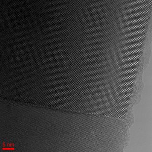
The LIBRA 200 CS TEM is based on the energy-filter version of the 200kV LIBRA TEM with a corrector for spherical aberrations of the objective lens. By use of this corrector, image resolution below 0.7 Angstrom can be achieved. Many applications will benefit from this development, e.g. imaging of interfaces in semiconductors or solar cells, grain boundaries in steel alloys or damage induced by nuclear radiation in shielding materials. In all these application fields the control of the material at the atomic scale is necessary for in-depth understanding of the underlying physical or chemical processes and to guarantee the functionality of the devices. Another advantage based on the CS corrector is the ability to reduce the acceleration voltage down to 80kV and still achieve resolutions below one Angstrom. Beam damage can thus be reduced and sensitive materials like carbon nanotubes can be analyzed.
The LIBRA 200 STEM with a corrector for the condenser system is used for imaging in the scanning mode with a resolution far below one Angstrom and extreme high resolution chemical analysis of samples, especially by means of electron energy loss spectroscopy (EELS). The corrected condenser allows minimizing the probe size below one Angstrom, and at the same time increases intensity. Additionally the unique monochromator reduces the energy spread down to 0.15 eV. Basic research in materials science (e.g. chemical analysis of nano-particles) especially will benefit from the resulting energy resolution that otherwise can only be reached at synchrotron rings.
“We have already started installation of several systems at customer sites in leading research facilities worldwide. Here resolution of 0.66 Angstrom could be demonstrated. Customer feedback is extremely positive,” explains Thomas Albrecht, Head of Product Management at Carl Zeiss SMT´s Nano Technology Systems division. “We do have a lot of experience with corrected transmission electron microscopes from customer specific installations like the CRISP system at the Caesar—Center for Advanced European Studies and Research in Bonn. Now we are using this experience to broadly offer this superb technology to the market. This strategy is in-line with our mission “Maximum Information—Maximum Insight.”
Correctors are developed and produced by the Heidelberg-based company CEOS GmbH, a specialist for electron optical correctors and a long-term partner for Carl Zeiss.