In the late 1990s, Dr. Thomas Zettler and a team around him developed and patented the first real-time epitaxy monitoring tool based on reflectance anisotropy spectroscopy - the Epi- RAS®. In October 1999, LayTec was founded as a spin-off of the Technical University of Berlin. Today, we provide the most advanced solutions for monitoring MOVCD, MBE and other thin- film growth processes. Since 2006 the application range of LayTec‘s in-situ monitoring systems has been expanded also to amorphous and organic thin-film growth processes (e.g. sputter deposition, VTE, OVPD).
 Laytec's new offices
A step to the photovoltaic market
In 2008, LayTec realized a strong demand from CIGC and CdTe based solar cell producers. After less than a year, the first orders were signed for SolR - LayTec‘s first in-line monitoring system for photovoltaic thin-film application. Now LayTec is cooperating with numerous partners to further develop the cuttingedge metrology solutions for the complete range of photovoltaic thin-film processes. Today, 2/3 of our equipment are in production line applications for LEDs! Good reasons to look back on 10 years of ongoing success.
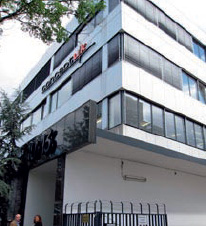
New premises
Just in time for our anniversary, we are moving to the new office that is twice as large as the current facilities. Now LayTec has more labs for research and development, larger rooms for production and quality control, for customer seminars and hands-on trainings. Please note our new address: Seesener Str. 10–13, 10709 Berlin.
Join us for the birthday party!
On October 9 we will celebrate our 10th birthday and cordially invite our customers and friends to join us! The party will be held in the spirit of Germany‘s traditional „Oktoberfest“ in a marquee in the backyard of the new office: a barbecue, beer and a live band will make sure that the party goes with a swing! Please let us now if you will join us on 9 October (5–10 p.m.) by sending an email to [email protected] before September 10.