The Pacific Northwest National Laboratory (PNNL), located in Richland, Washington, is bringing an ORION® PLUS instrument into the U.S. Department of Energy's Environmental Molecular Sciences Laboratory as a resource. And, in Tsukuba, Japan, the National Institute of Advanced Industrial Science and Technology (AIST) has selected an ORION PLUS for their new Nanodevice Innovation Research Center. These installations provide further evidence of a growing reliance on helium-ion microscopy for the most demanding research in materials, life science and semiconductor applications.
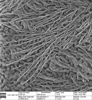 One of EMSL’s priorities is to research mineral to mineral and mineral to microbial filaments. This ORION image shows mineral filaments interpenetrating porous silicon. Even though the uncoated, insulating sample suffered from charging when imaged by a scanning electron microscope (SEM), the helium-ion microscope produced superior resolution images with no charging problems.
PNNL has become the first US national lab to acquire a ZEISS ORION PLUS helium-ion microscope. One of the Department of Energy's (DOE's) ten national laboratories, managed by DOE's Office of Science, PNNL offers an open, collaborative environment for scientific discovery to researchers around the world. “We are very excited to be adding a helium-ion microscope to our arsenal of leading-edge scientific instruments,” said Shuttha Shutthanadan, scientist at the Environmental Molecular Sciences Laboratory (EMSL), a national scientific user facility located at PNNL. “Basically, helium-ion microscopy improves our vision at the nanoscale, allowing us to see things we could never see before. Having access to an instrument that provides world-record spatial resolution imaging, plus high image contrast and large depth of field will enable our users to accelerate their innovations.”
Weilin Jiang, EMSL scientist, adds, “Perhaps one of the greatest advantages of helium-ion microscopy is the ability to clearly image uncoated insulating materials.” This circumvents the time consuming, resolution diminishing practice of coating a sample to deal with its charging. The tool is scheduled for delivery at the end of March of this year.
At the prestigious AIST in Tsukuba, Japan, formal acceptance of their new ORION PLUS microscope was completed on February 8 of this year. The AIST system is outfitted with all of the available options, including the recently developed Spectra Detector. A newly designed Gas Injection System will be added shortly. “Installation and acceptance were completed rapidly and without any major issues, including a dramatic trip by crane to a fourth floor balcony of the AIST building,” reports David Voci, Carl Zeiss SMT's director of business development for the ORION product. AIST will use the tool in support of their research into next generation semiconductor technology, as well as for clean energy applications.
Research topics identified include Low K dielectrics, EUV photomask metrology, nano- imprint lithography, carbon nanotube and graphene device research, as well as applications in support of solar and fuel cell research. The instrument is situated in a user facility that eventually will be available to all AIST researchers for a broad range of uses from semiconductor to life science applications. “The AIST system was the first ORION PLUS microscope delivered that was designed and built to achieve the 0.35nm probe size specification. The EMSL ORION PLUS instrument is the second tool of this generation, and we are confident that our production and field service team will accomplish this installation equally well as with the AIST system,” comments Voci.