Researchers at imec have developed an innovative strategy to tune plasmon resonances. They do so by breaking the symmetric geometry of the nanostructures, using a combination of bottom-up and top-down fabrication processes. Such broken symmetry can lead to strongly enhanced local electric fields. A potential application is the detection of biomolecules via surface-enhanced Raman scattering (SERS).
Metal-based nanophotonics (plasmonics) is a field concerned with manipulating and focusing light on nanoscale structures that are much smaller than conventional optic components. Plasmonic technology, today still in an experimental stage, has the potential to be used in future applications such as nanoscale optical interconnects for high performance computer chips, highly efficient thin-film solar cells, and extremely sensitive (bio)molecular sensors.
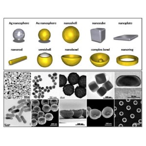 (top) Schematic illustration of various shapes of plasmonic nanostructures and (bottom) the corresponding electron microscopy images.
Plasmonic applications can be made from nanostructured (noble) metals. When such nanostructures are illuminated with visible to near-infrared light, the excitation of collective oscillations of conduction electrons - called surface plasmons - generates strong optical resonances, focusing electromagnetic energy in deep-sub-wavelength-scales. The resonance spectra of the metallic nanostructures strongly depend on their geometry. Imec has extensive experience in synthesizing various shapes of nanostructures to tune the resonances from the ultraviolet to the near-infrared region. Examples of such shapes are nanospheres, nanocubes, nanorods, nanoshells, and nanorings.
Recently, researchers at imec have developed an innovative strategy to precisely tune the plasmon resonances. They do so by breaking the symmetric geometry of the nanostructures, using a combination of bottom-up and top-down fabrication processes. This allows making a geometrical transition from nanocubes to nanoplates (see Jian Ye, et al. Nanotechnology, 2008, 19, 325702), from nanoshells to semishells and nanobowls (see Jian Ye, et al. the Journal of Physical Chemistry C, 2009, 113, 3110; Jian Ye, et al. Langmuir, 2009, 25, 1822; Jian Ye, et al. ACS Nano, 2010, 4, 1457), from nanocages to open-nanocages (see Jian Ye, et al. Optics Express, 2009, 17, 23765).
Combining bottom-up and top-down fabrication turns out to be a cost-effective method to obtain large areas covered with engineered metal nanostructures. The nano-dimensions are still set by the bottom-up fabrication procedures, and the geometrical tweaking occurs through well-characterized top-down fabrication techniques such as metal evaporation and ion milling.
Imec has gained a substantial insight in the optical properties of these nanostructures using a combination of electromagnetic simulations and advanced optical spectroscopy. This allows explaining the optical properties using the so-called plasmon hybridization model, where the resonances of complex nanostructures can be described as bonding and anti-bonding arrangements of the parent plasmon resonances of the individual constituents. This paves the way to tweaking the optical properties of metal nanostructures for various applications. More specifically, the broken symmetry can lead to strongly enhanced local electric fields, which show a potential application in surface-enhanced Raman scattering-based bio-molecular detection.