Imec and Holst Centre have developed an innovative sensor for measuring ultra-low concentrations of NO2. Such sensors are important for applications that monitor environmental pollution resulting from traffic, and in general, from all combustion motors.
The sensor’s active components are arrays of grown vertical InAs nanowires. A typical sensor would contain 500 such nanowires, and will be sensitive to NO2 concentrations of fewer than 100ppb at room temperature.
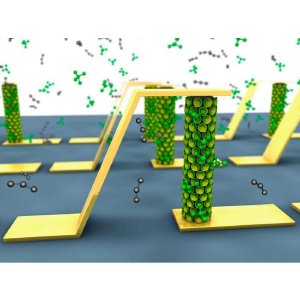 Artist impression of the NO2 gas sensor, showing the contacts and InAs nanowires.
The sensor’s nanowires are about 3µm in length and 50-100nm wide. They are made from InAs, which is well-suited for gas sensing, because it has an electron accumulation layer at the surface, making it sensitive to accumulated charges. Gas molecules adsorb onto the nanowires, changing the current that is flowing through the nanowires.
The semiconductor nanowires are contacted ohmically using an air bridge construction (see picture). This construction has as advantage that it leaves the nanowire surface free for gas adsorption. Because of the small bandgap of InAs, it’s fairly easy to fabricate these ohmic contacts. The sensor can be reset, simply by applying a stronger current.
The new sensor boasts several breakthroughs in nanowire technology. A key characteristic is that the vertical nanowires are electrically contacted in the locations on the substrate where they are grown. In other, comparable nanowire sensors, the nanowires have to be placed on the substrate after being grown elsewhere. Another major benefit of these sensing nanowires is that they function without heating, making them much more power-efficient.
The new gas sensor has been developed in Holst Centre’s program for ultra-low-power sensors. In a next step, the researchers will increase the sensitivity of the sensor, as well as its detection selectivity. One goal is, for example, to make a sensor that can distinguish between NO2 and NO. Also, new manufacturing techniques are investigated, with the aim to use cost-effective silicon substrates for high-yield solutions.