Imec has derived a process flow concept for the packaging of medical implants that meets the requirements for miniaturization, biocompatibility and safety. The proposed solution is a promising alternative for the currently used rigid packages that tend to enhance foreign body reactions.
The technological developments within the field of electronics have allowed for a significant downsizing of active medical devices. In order to take full advantage of this miniaturization, the housing/packaging of the devices should keep pace with these developments. Imec now proposes a process flow for packaging active medical implants allowing for further miniaturization and taking into account the stringent requirements for biocompatibility and safety. The latter include hermetic sealing to protect the human body, protection of the device from seeping of bodily fluids into the implant, biocompatibility (putting requirements on the chemical composition, shape and mechanical properties of the package) and suitability for the required standard sterilization technique.
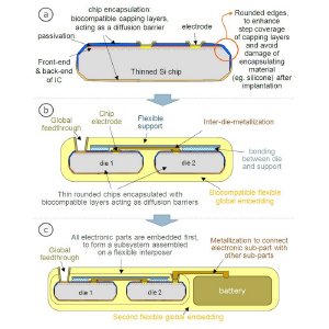 (a) Scheme of biocompatible chip encasulation and (b & c) possible basic concept of an implantable system consisting of thin dies encapsulated with biocompatible bi-directional diffusion barriers. In case (b), only electronics and metallization is embedded, in case (c) a second embedding is used to combine the electronic sub-part of the device with other parts such as a battery.
An active implantable device typically consists of various sub-devices, i.e. a CMOS chip, a microsystem, a battery, electric components, a drug reservoir, a sensor, a microfluidic device etc. All sub-devices are electrically connected with each other and sometimes electrodes are also in direct contact with the human body.
The first phase of the process flow involves the hermetic encapsulation of all individual dies. For this step, imec proposes a wafer-level based processing that is carried out by using conventional cleanroom tools. It is realized by encapsulating the topside of the chips after (partial) wafer dicing, followed by mounting the wafer upside down on a carrier for wafer thinning and a second encapsulation step from the chip backside. The encapsulation layers serve as biocompatible bi-directional diffusion barriers and can be made from various materials such as Si (or Ti) oxide, Si (or Ti) nitride, Si carbide etc. A sloped sawing technique is used to make sloped chip edges, ensuring a better step coverage of the capping layers. As a proof of concept, the obtained diffusion barrier properties of a Si oxide/nitride based encapsulation layer is illustrated by cell culture tests.
The second phase of the packaging consists of the assembly of sub-devices, the fabrication of interconnects using a biocompatible metallization technique, and the global embedding in a soft flexible material. This phase is often split into two parts: firstly, the electronic chips will be embedded resulting in a kind of interposer, followed by a second global embedding of this interposer together with other non-Si based subparts (e.g. battery, passives) of the total system. The global embedding is typically a board-level process since larger interconnect pitches have to be realized. The fabrication of the interposer-like package to embed Si dies might be carried out using board-level or wafer-level technologies. Cost plays an important role in the selection of the technology. However, imec’s fabrication cost calculations have demonstrated that the dominant factor in the cost of a biocompatible packaging is given by the metallization process. Noble metals such as platinum show excellent biocompatibility but their metallization is very expensive. This second phase of the packaging process, including the development of an optimized and cost-effective metallization scheme, is the subject of ongoing research.
The proposed solution is a promising alternative to the existing titanium or ceramic based packages. Titanium/ceramic packaged implants are large and rigid, enhancing the foreign body reaction and preventing further miniaturization.
These results have been proposed in more detail during the Electronics System Integration Technology Conference (ESTC) 2010.