At the International Workshop on Nitride Semiconductors (IWN) in Switzerland on 6–10 October, Prof. Misaichi Takeuchi of the Ritsumeikan University, Japan, presented in-situ curvature measurements gained with LayTec‘s EpiCurve®R TT metrology system on AIXTRON 200 RF-S MOCVD reactor.
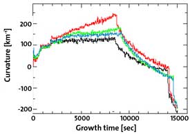 Fig. 1: Curvature measurements:
black curve - 1 step growth TMAl pre-treatment of 0 sec;
red curve - 1 step growth TMAl pre-treatment of 150 sec;
green curve - 2 step growth, TMAl=0 sec, NH3 during annealing;
blue curve - 2 step growth, TMAl=0 sec, without NH3 during annealing
Fig. 1: Curvature measurements:
black curve - 1 step growth TMAl pre-treatment of 0 sec;
red curve - 1 step growth TMAl pre-treatment of 150 sec;
green curve - 2 step growth, TMAl=0 sec, NH3 during annealing;
blue curve - 2 step growth, TMAl=0 sec, without NH3 during annealing
The sensor combines wafer bowing, temperature and growth rate monitoring with spectroscopic reflectance measurements. Prof. Takeuchi and his team used the measurement system to develop a new growth method for crack-free thick AlN layers on sapphire and of n-AlGaN on AlN/sapphire in order to optimize AlGaN-based deep UV emitters and high-voltage AlGaN/AlGaN HEMTs.
For these devices the simplest way to improve the layer quality, i.e. to reduce XRD FWHM values, is to grow thicker layers. At the same time, cracking caused by strain relaxation at critical thickness has to be avoided. To control the strain, Prof. Takeuchi used EpiCurve®R TT to monitor wafer curvature, spectroscopic reflectance (λ=330–750 nm) and the real wafer temperature simultaneously. The measurements enabled him to follow the nano-scale surface-morphological evolution and to understand the influence of AlN growth parameters on the critical thickness.
This work showed that the Al-polar oriented growth had a tendency to enhance wafer bowing and film stress, whereas N-polar growth did not. With this knowledge, Prof. Takeuchi developed a new two-step growth procedure consisting of pre-treatment stages with NH3 or TMAl to control the surface polarity, seed layer growth, annealing and overgrowth stages for generating low-strain Al-polar films.
Fig. 1 shows the curvature data of samples with the single-step growth with TMAl pre-treatment of 0 sec (including some Npolar grains) and 150 sec (completely Al-polar), and the two-step growth with and without NH3 during annealing of the TMAl = 0 sec seeding layers. The surface polarity of both twostep growth samples have been unified to Al-polar. However, the strain in both samples is effectively reduced compared with the Al-polar sample of TMAl=150 sec. Hence, low-strain AlN films with Al-polar surface have been formed. Furthermore, the research showed that (002) and (102) XRD FWHM values were drastically improved by the two-step growth.
At the IWN, Prof. Takeuchi also presented the results of growth of AlN layers inserted beneath highly doped AlGaN layers on sapphire. In this case, wafer bowing and cracking are serious problems because highly Si-doped n-AlGaN layers enhance concave bowing. EpiCurve®R TT detected the related doping-induced accumulation of tensile stress. Prof. Takeuchi could directly correlate this effect to ex-situ XRD FWHM values.