Apr 9 2009
Since the advent of copper damascene processing, achieving void-free fill of high aspect ratio interconnect features has been a key challenge for device manufacturers. Shrinking dimensions at each successive technology node have increased the complexity of the copper seed and electroplating processes, and stringent yield and reliability requirements have intensified the focus on reducing defects.
 Novellus' Suppression-Enhanced Fill(TM) Technology Provides Defect-Free 32nm Copper Interconnects
Copper interconnect defects can be caused by a multitude of factors, including post-patterning etch residue, discontinuous barrier or seed layers, and inadequate electroplating nucleation and deposition. Overcoming these interconnect scaling challenges is paramount to increasing memory bit density, shrinking chip form factor and enhancing circuit functionality. Device manufacturers need solutions to these problems to enable the next generation of consumer-driven applications such as solid state drives and smart phones.
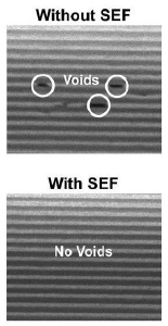
To address the manufacturing challenges associated with advanced copper interconnects, Novellus (NASDAQ:NVLS) researchers have developed an innovative copper electrochemical process called Suppression-Enhanced Fill(TM) (SEF) that eliminates defects when scaling to the 32nm technology node. The SEF process utilizes unique capabilities of the company's SABRE(R) Extreme platform to simultaneously enhance current suppression on the wafer field and within the upper sidewalls of contacts and trenches while permitting copper deposition to initiate rapidly from the bottom of these features. In addition, SEF increases fill nucleation density and decreases the possibility of seed dissolution, resulting in copper electrofill that is easier to integrate with today's barrier and seed technologies. Figure 1 shows 32nm features filled using the SEF process, resulting in a more robust, void-free fill.
"With SEF, our goal is to provide a new electroplating process that allows our customers to transition to the 32nm technology node with minimal process changes and capital expenditure," said Dr. Andrew McKerrow, director of technology for the company's Electrofill business unit. "SEF has been adopted by our leading edge memory and logic customers for their 32nm technology node and is already a key part of the effort to extend Cu interconnects to 2Xnm."