Jul 16 2010
University of Illinois engineers have developed a novel direct-writing method for manufacturing metal interconnects that could shrink integrated circuits and expand microelectronics.
Integrated chips are made by wiring multiple transistors and electronic components together to perform complex functions. The connections between chips and circuit boards traditionally are made from pre-fabricated metal wires that connect to a designated bonding pad on a chip.
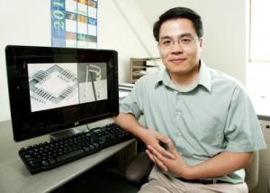
"Integrated functions require many wire connections. It's tedious and time-consuming to make and increases cost," said Min-Feng Yu, a professor of mechanical science and engineering at Illinois.
 University of Illinois engineers have developed a novel direct-writing method for manufacturing metal interconnects that could shrink integrated circuits and expand microelectronics.
In addition, the bonding pad for traditional wire bonds takes up a substantial area of space. As technology has moved toward smaller electronics, shrinking wiring has been a substantial obstacle. Many microelectronic devices are much smaller than the required 50-by-50 micron square bonding site, prohibiting integrated functions on the very small scale.
"There's no existing cost-effective technology that would allow you to wire-bond microstructures," said Yu, "so let's get rid of those wires, and instead, why not directly produce them on-site between the connection points?"
Yu and graduate student Jie Hu developed a direct-write technique that produces tiny pure metal wires much smaller in diameter than traditional wires and requiring two orders of magnitude less bonding area. In a paper appearing in the July 16 edition of Science, they demonstrate as many as 20 of their new wires bonded to a single standard bonding site.
"This technique means the pads can be much smaller than what's needed for traditional wire-bonding technology," Yu said. This reduction in area could allow manufacturers to produce more chips per wafer of semiconductor material. It could also enable more complex integrated functions in microelectronics.
The pair have demonstrated their technique with both copper and platinum wires, and plan to explore the technique with other metals.
Yu likens their technique to writing with a fountain pen. "People's mindset is that you draw a line on a surface, but what we're doing is writing to 3-D space," he said.
The duo loaded a micropipette – a device that dispenses tiny amounts of liquid – with a copper electrolyte solution. When the pipette comes into close contact with the surface, a liquid bridge forms between the pipette tip and the bonding pad. The researchers then apply an electric current, which causes the copper in the solution to deposit as solid metal. As the tip moves through space, copper continues to deposit from the solution in the pipette, like ink from a pen, creating a wire. The challenge for Yu and Hu was calculating the correct speed to move the pipette tip to maintain the liquid bridge between the nozzle and the growing wire.
"It's liquid, so it can easily be shaped," Yu said. "As long as you maintain your speed within a certain range, you will always be able to produce uniform, high-quality wires."
They also had to figure out how to "write" the wires laterally for chip-to-chip bonding. Typical micropipette nozzles are flat at the end, but too much tilting breaks the liquid contact. The Illinois duo found that a notched nozzle, with a 90-degree cut in the side, allowed lateral movement, meaning that the wires can arc from one bonding site to another, even if the chips are stacked or tiered.
The process is automated, so Yu hopes to develop arrays of micropipettes to produce wire bonds in bulk for more efficient manufacturing.
"An advantage is that you can do this in parallel," he said. "Instead of one nozzle, suppose you have 10, 20 or 100 working simultaneously. In one step, you can make tens or hundreds of bonds, and that is cost-saving."
In addition to wire bonds, the technique could produce a myriad of metal microstructures for various applications.
"The ability to fabricate metallic structures in 3-D can open up many other opportunities," Yu said. "It has lots of desirable properties aside from the electrical ones. You can imagine the structures that take advantage of the different properties of metal."
Source: http://illinois.edu/