Feb 23 2011
NEC Corporation (NEC; TSE: 6701) announced today the successful demonstration of a low power programmable cell array using a rewritable and nonvolatile solid-electrolyte switch, "NanoBridge(R)," integrated into a 90nm CMOS.
NanoBridge is the resistive switch where resistance changes between ON and OFF states when a nanometer scale Cu bridge is precipitated or dissolved into the solid electrolyte. When placed between the two Cu interconnects of LSI, NanoBridge can connect or disconnect the two interconnects by applying a bias voltage. Therefore, circuitry can be configured after manufacturing in order to implement logic functions. Each NanoBridge state is nonvolatile and it maintains its resistive state without power dissipation.
 Chip Comparison
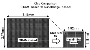
This new technology features a programmable switch equipped with NanoBridge that is monolithically stacked on programmable logic circuits composed of transistors. The electrical properties of NanoBridge, such as the distribution of turn-on voltage, have been improved by introducing a newly developed PSE (polymer solid-electrolyte). These technologies have reduced chip size by 1/4 and reduced dynamic power consumption by 1/4 when compared to a reference programmable array using SRAM (static random access memory) based switches.
These latest NanoBridge developments feature the following:
-
The programmable switch plane is monolithically stacked on the logic plane, which results in a 1/4 chip size reduction and a 1/4 reduction in dynamic power consumption when compared with conventional technology.
The switch plane is composed of NanoBridges that configure LSI interconnects and NanoBridges that configure the logic circuit. The logic plane features newly developed programmable logic from NEC that has the same functionality as conventional programmable logic even though it is smaller in size. This is due to the substantial number of NanoBridges in the switch plane. As a result, both the chip size and dynamic power have been reduced by 1/4 when compared to the conventional programmable array with SRAM-based switches.
-
The distribution of NanoBridge electrical properties has been improved by introducing a newly developed solid-electrolyte, PSE.
The uniform formation of a nanometer scale Cu bridge results in a more narrow distribution of turn-on voltage. This leads to the successful programming of a 32x32 crossbar switch without select transistors in the logic plane, which eliminates the need for additional area due to NanoBridges in the logic plane.
Currently, cloud computing is becoming increasingly widespread, and a larger number of transactions are being processed by computer and communications tools. As a result, managing the power of these instruments has become a serious challenge, where it is necessary to preserve the quality of computing while decreasing the power consumption of Si chips.
Transactions processed by a CPU (central processing unit) require more power and computing time than transactions processed by hardware such as an accelerator chip, which is specialized for processing specific transactions.
This innovative low power programmable array helps to reduce the power consumption of instruments by processing different kinds of transactions through the reconfiguration of circuits, which enables lower power consumption and shorter computing times.
These newly developed technologies are a result of NEC's long-time development of NanoBridge technology, which enabled the first time successful operation of low power programmable cell arrays. Looking forward, NEC will continue to promote the development of innovative new programmable devices.
NEC will present these NanoBridge based programmable cell array achievements at the International Solid-State Circuit Conference (ISSCC) held in San Francisco from February 20, 2011. NEC will present NanoBridge technologies on February 22.
A portion of this work was supported by the Ministry of Economy, Trade and Industry (METI) and the New Energy and Industrial Technology Development Organization (NEDO) as part of the Project of Strategic Development for Energy Conservation Technology.
Source: http://www.nec.co.jp/