U.S Scientists have produced a very small optoelectronic device by folding a nanoscale wafer of aluminium oxide, comprising a gold pattern on its surface, into a hollow cube. They have produced a very small three-dimensional split-ring resonator, which is widely used in metamaterials and exhibits peculiar electronic and physical properties.
The scientists state that the three-dimensional device offers better functioning than its two-dimensional counterpart and enables the production of functional and accurately engineered devices at the nanoscale.
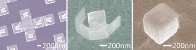 nanobox
David Gracias with his colleagues at Johns Hopkins University, US, demonstrated how nanoscale origami is applied to fold a sheet into a cube. This process is being taken one step forward by functionalizing the product.
The first step in making the cube is depositing a layer of polymethylmethacrylate upon a silicon substrate. Using electron beam lithography, a mould was carved into a cruciform shape to form the final cube with six sides. Then, aluminium oxide is filled into the mould. Polymer is deposited as a second layer. To form the box hinges, a portion of the polymer at the junction point of the individual panels is cut off and filled with tin. Polymer is later separated and by using activated fluorine, the silicon is cut off. Tin is melted by the heat energy released due to this exothermic reaction. The melted tin combines together and generates twisting forces that folds the alumina panels towards inside forming a cube. In order to impart optoelectronic properties to a split-ring resonator, the pattern’s surface was coated with gold prior to covering the cube's panels.
Gracias suggested that particle making is quite simple in nanotechnology, but creating patterns for it, is a tough task. This process costs more and only a few structures can be created at a time, he added.
Mark Morrison, chief executive, UK educational charity, the Institute of Nanotechnology, stated that the combination of bottom-up self assembly methods and top-down techniques such as lithography and deposition has gained importance. These devices can be applied in various fields from medicine to computing. This research still requires a lot of improvement before applying it in real life usage, added Morrison.