Photolithography is a common method for producing computer chips. But the visible light wavelength reduces the transistor’s size produced using this method.
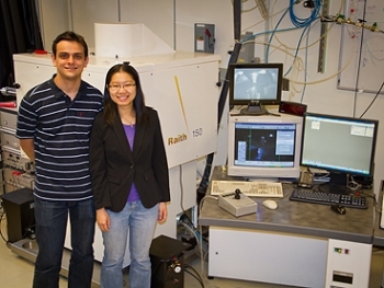 electron-beam lithography system used by MIT research team
To overcome this problem, researchers used a technique called electron-beam or e-beam lithography to produce prototype chips. But the traditional e-beam lithography method is much slower than photolithography.
e-beam lithography uses the same general approach as that of a ultraviolet and visible-light. The materials involved in chip making are made to pile up in layers. Each time a layer is deposited, a material referred to as resist is used to cover the layer. The resist is then exposed to light or a beam of electrons in a set pattern. The resist and the layer below it that are not exposed to light are removed off; on the other hand, the resist that is exposed to light shields the material it covers. Repeat process of this slowly builds up three-dimensional structures on the surface of the chip.
In the e-beam lithography process, the electron beam hits the resist surface row-by-row and hence consumes more time. The efficiency of e-beam lithography can be improved by using multiple electron beams at a single shot, but how long a beam has to stay on the resist surface is a big question. MIT researcher’s work provided a solution to this problem.
RLE research team identified two ways to enhance the resolution of high-speed e-beam lithography. The first way was to make use of a slimmer resist layer that helps to reduce electron scattering. The other way was to create the resist using a solution that contains common salt and hardening the areas that are hit by more number of electrons leaving the areas that receive fewer electrons.
Source: www.mit.edu