Feb 2 2013
A new way of growing graphene without the defects that weaken it and prevent electrons from flowing freely within it could open the way to large-scale manufacturing of graphene-based devices with applications in fields such as electronics, energy, and healthcare.
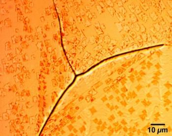 Optical micrograph showing graphene domains formed across grain boundaries.
A team led by Oxford University scientists has overcome a key problem of growing graphene – a one atom-thick layer of carbon – when using an established technique called chemical vapour deposition, that the tiny flakes of graphene form with random orientations, leaving defects or 'seams' between flakes that grow together.
The discovery, reported in a paper to be published in ACS Nano, reveals how these graphene flakes, known as 'domains', can be lined up by manipulating the alignment of carbon atoms on a relatively cheap copper foil – the atomic structure of the copper surface acts as a 'guide' that controls the orientation of the carbon atoms growing on top of them.
A combination of control of this copper guide and the pressure applied during growth makes it possible to control the thickness of these domains, the geometry of their edges and the grain boundaries where they meet – 'seams' that act as obstacles to the smooth progress of electrons necessary to create efficient graphene-based electrical and electronic devices.
'Current methods of growing flakes of graphene often suffer from graphene domains not lining up,' said Professor Nicole Grobert of Oxford University's Department of Materials who led the work. 'Our discovery shows that it is possible to produce large sheets of graphene where these flakes, called 'domains', are well-aligned, which will create a neater, stronger, and more 'electron-friendly' material.'
In principle the size of the sheet of graphene that can be created is only limited by the size of the copper base sheet.
The Oxford-led team, which includes researchers from Forschungszentrum Juelich Germany, the University of Ioannina Greece, and Renishaw plc, has shown that it is also possible using the new technique to selectively grow bilayer domains of graphene – a double layer of closely packed carbon atoms – which are of particular interest for their unusual electrical properties.
'People have used copper as a base material before, but this is the first time anyone has shown that the many different types of copper surfaces can indeed strongly control the structure of graphene,' said Professor Grobert. 'It's an important step towards finding a way of manufacturing graphene in a controlled fashion at an industrial scale, something that is essential if we are to bridge the gap between fundamental research and building useful graphene-based technologies.'
Source: http://www.ox.ac.uk