Dec 22 2014
An atomically thin material developed at Rice University may lead to the thinnest-ever imaging platform.
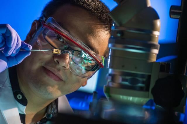 Rice University graduate student Sidong Lei displays a three-pixel prototype made with atomically thin layers of CIS. The new material developed at Rice shows promise for two-dimensional electronics. (Credit: Jeff Fitlow/Rice University)
Synthetic two-dimensional materials based on metal chalcogenide compounds could be the basis for superthin devices, according to Rice researchers. One such material, molybdenum disulfide, is being widely studied for its light-detecting properties, but copper indium selenide (CIS) also shows extraordinary promise.
Sidong Lei, a graduate student in the Rice lab of materials scientist Pulickel Ajayan, synthesized CIS, a single-layer matrix of copper, indium and selenium atoms. Lei also built a prototype -- a three-pixel, charge-coupled device (CCD) -- to prove the material's ability to capture an image.
The details appear this month in the American Chemical Society journal Nano Letters.
Lei said the optoelectronic memory material could be an important component in two-dimensional electronics that capture images. "Traditional CCDs are thick and rigid, and it would not make sense to combine them with 2-D elements," he said. "CIS-based CCDs would be ultrathin, transparent and flexible, and are the missing piece for things like 2-D imaging devices."
The device traps electrons formed when light hits the material and holds them until released for storage, Lei said.
CIS pixels are highly sensitive to light because the trapped electrons dissipate so slowly, said Robert Vajtai, a senior faculty fellow in Rice's Department of Materials Science and NanoEngineering. "There are many two-dimensional materials that can sense light, but none are as efficient as this material," he said. "This material is 10 times more efficient than the best we've seen before."
Because the material is transparent, a CIS-based scanner might use light from one side to illuminate the image on the other for capture. For medical applications, Lei envisions CIS being combined with other 2-D electronics in tiny bio-imaging devices that monitor real-time conditions.
In the experiments for the newly reported study, Lei and colleagues grew synthetic CIS crystals, pulled single-layer sheets from the crystals and then tested the ability of the layers to capture light. He said the layer is about two nanometers thick and consists of a nine-atom-thick lattice. The material may also be grown via chemical vapor deposition to a size limited only by the size of the furnace, Lei said.
Because it's flexible, CIS could also be curved to match the focal surface of an imaging lens system. He said this would allow for the real-time correction of aberrations and significantly simplify the entire optical system.
Source: http://www.rice.edu/