Apr 24 2015
The characterization technology needed for nanoelectronic materials and device research, development, and manufacturing was discussed by experts from industry, government, and academia at the 2015 International Conference on Frontiers of Characterization and Metrology for Nanoelectronics (FCMN), which was held in Dresden, Germany, on April 14-16, 2015.
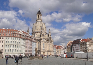
 Dresden
Many of the presentation slides and posters are available to view on the conference website.
A city of notable art treasure, architectural sights, and a charming landscape, Dresden also has the largest hub of microelectronics in Europe. Dresden is a center of microelectronics manufacturing, with Globalfoundries, Infineon, and others located within or near the city. In addition, research and development takes place at the nearby Fraunhofer Institutes and the Technische Universität Dresden.
As the devices lying at the heart of computing shrink ever closer to fundamental limits, the semiconductor industry is confronting the problem of what to do when conventional microprocessors simply cannot shrink any further. The bi-yearly conference is an ideal event for anyone concerned about the future of characterization and metrology for semiconductor manufacturing—a ≈$340 billion industry.
Highlights from the 2015 FCMN included three successive keynote addresses which opened the conference by Hubert Lakner, Executive Director, Fraunhofer Institute for Photonic Microsystems; Suresh Venkatesan, Senior Vice President, Technology Development, Global Foundries; and Nobel Prize winner Klaus von Klitzing, Max-Planck-Institut FKF.
“Suresh Venkatesan provided an excellent overview of what’s driving the semiconductor industry and what’s driving the excitement in the industry,” states David Seiler, Chief of PML’s Semiconductor and Dimensional Metrology Division and Co-Chair of the conference. “He described a pervasiveness of metrology in the fab. Fifty percent of all steps in the fab are metrology related and this is growing. Twenty-five to thirty percent of all tools in the fab are metrology related. And 3D metrology is increasing.
“The conference was a resounding success,” says Seiler. “We had over 140 attendees, and everyone was extremely pleased with the technical content and looks forward to the next conference in two years!”
Source: http://www.nist.gov/