Feb 4 2016
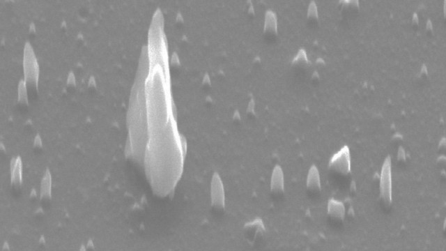 Scanning electron micrograph of c-BN nanoneedles and microneedles up to three microns in length. Image credit: Anagh Bhaumik.
A team of researchers from North Carolina State University have determined a new phase of boron nitride (Q-BN), which plays a vital role in both electronic displays and manufacturing tools. The team have come up with a new method for forming cubic boron nitride (c-BN) at ambient air pressure and temperatures. This method is used for a wide range of application, such as the develop,emt modern power grid technologies.
This is a sequel to our Q-carbon discovery and converting Q-carbon into diamond. We have bypassed what were thought to be the limits of boron nitride’s thermodynamics with the help of kinetics and time control to create this new phase of boron nitride. We have also developed a faster, less expensive way to create c-BN, making the material more viable for applications such as high-power electronics, transistors and solid state devices. C-BN nanoneedles and microneedles, which can be made using our technique, also have potential for use in biomedical devices.
Jay Narayan, John C. Fan Distinguished Chair Professor of Materials Science and Engineering, NC State
C-BN, a type of boron nitride, has a cubic crystalline structure, similar to diamond.
The tests that were previously conducted highlighted that Q-BN, when compared with diamond, is harder and more efficient when forming cutting tools. Diamond reacts with ferrous materials and iron just like that of carbon, but Q-BN does not. The Q-BN has an indefinite structure, and is used to coat cutting tools in an easy manner, preventing the tools from causing any reactions with ferrous materials.
We have also created diamond/c-BN crystalline composites for next-generation high-speed machining and deep-sea drilling applications. Specifically, we have grown diamond on c-BN by using pulsed laser deposition of carbon at 5,000 degrees Celsius without the presence of hydrogen, creating c-BN and diamond epitaxial composites.
Jay Narayan, John C. Fan Distinguished Chair Professor of Materials Science and Engineering, NC State
When exposed to extremely low electrical field levels, the Q-BN glows in the dark due to its negative electron affinity and low work function. These features make Q-BN an efficient material for energy-efficient display technologies.
The researchers started the Q-BN development process using a thermodynamically stable layer of hexagonal boron nitride (h-BN), which can have a thickness of up to 500-1000 nm. After placing the material on a substrate, the researchers heat the h-BN to 4,580°F, or 2,800 K in a rapid manner, using high-power laser pulses. A substrate capable of swiftly absorbing heat is used to quench the material. This entire technique is executed at ambient air pressure, and takes almost one-fifth of a microsecond.
Researchers can monitor whether h-BN is transformed into c-BN or Q-BN by controlling the seeding substrate placed below the material, and manipulating the time taken to cool the material. The same variables can help decide whether the c-BN develops into a film, microneedles, microcrystals, nanodots, and nanoneedles.
Using this technique, we are able to create up to a 100- to 200-square-inch film of Q-BN or c-BN in one second.
Jay Narayan, John C. Fan Distinguished Chair Professor of Materials Science and Engineering, NC State
Previously c-BN was formed by heating hexagonal boron nitride to 500 K (5,840°F), and using 95,000 atmospheres of pressure.
Though C-BN and diamond have very similar properties, it should be noted that C-BN has many advantages over diamond. c-BN has an attractive higher bandgap, which is used in high-power devices. c-BN can obtain negatively- and positively-charged layers by being doped, and can be used to create transistors. When exposed to oxygen, c-BN creates a firm oxide layer on its surface, enabling it to be sturdy at high temperatures. This final advantage demonstrates that c-BN can be used to develop protective coatings and solid state devices for high-speed machining tools utilized in oxygen-ambient environments.
We’re optimistic that our discovery will be used to develop c-BN-based transistors and high-powered devices to replace bulky transformers and help create the next generation of the power grid.
Jay Narayan, John C. Fan Distinguished Chair Professor of Materials Science and Engineering, NC State
The study results have been reported in APL Materials, under the title “Direct conversion of h-BN into pure c-BN at ambient temperatures and pressures in air.”
NC State Ph.D. student Anagh Bhaumik was the co-author of the paper. The National Science Foundation supported the work under grant DMR-1304607.