Feb 11 2016
A new transistor, capable of revolutionizing thin-film electronic devices, has been developed by an engineering research team at the University of Albert (U of A).
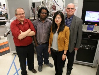 UAlberta electrical engineering PhD student Gem Shoute (second from right) is the lead author on a research paper demonstrating a powerful new flexible transistor. The team: electrical engineering professor Doug Barlage, Triranta Muneshwar, Shoute and materials engineering professor Ken Cadien, published its work in Nature Communications.
The team’s findings, published in Nature Communications, holds potential to develop flexible electronic devices with applications in diverse fields, such as medical imaging, display technology, and renewable energy production.
Initially they explored new applications for thin film transistors (TFT) that are often found in low-frequency, low power devices; including the computer display screen. Attempts by researchers and the consumer electronics industry to enhance the transistors performance have been hindered by the difficulties faced to develop new materials, or to enhance the existing devices for application in conventional TFT architecture, referred to as the metal oxide semiconductor field effect transistor (MOSFET).
The U of A electrical engineering team, instead of trying to develop new materials, improved the performance through a new transistor design architecture, taking into account the effect of bipolar action. Rather than employing a particular type of charge carrier used in most TFTs, the group utilized electrons and holes to provide the electrical output. The initial breakthrough was achieved by creating an ‘inversion’ hole layer in a ‘wide-bandgap’ semiconductor, a difficult task in the solid-state electronics field.
As soon as this was realized, “we were able to construct a unique combination of semiconductor and insulating layers that allowed us to inject “holes” at the MOS interface,” said Gem Shoute, a PhD student in the Department of Electrical and Computer Engineering who is lead author on the article. The addition of holes at the interface improved the likelihood of an electron “tunneling” through a dielectric barrier. With the help of this phenomenon, a form of quantum tunneling, they were able to create a transistor that behaved like a bipolar transistor.
It’s actually the best performing [TFT] device of its kind—ever. This kind of device is normally limited by the non-crystalline nature of the material that they are made of.
Ken Cadien, Materials Engineering Professor, U of A
The device’s geometries can be scaled with ease to enhance the performance and achieve miniaturization, a desirable feature that is missing in modern TFTs. The new transistor has 10 times more power-handling capabilities than the currently available TFTs.
Electrical engineering professor Doug Barlage, who is Shoute’s PhD supervisor and one of the paper’s lead authors, says his team was keen to develop new approaches. The researchers believed that a high-power TFT could be produced, finding out how was the question.
Our goal was to make a thin film transistor with the highest power handling and switching speed possible. Not many people want to look into that, but the raw properties of the film indicated dramatic performance increase was within reach. The high quality sub 30 nanometer (a human hair is 50 nanometers wide) layers of materials produced by Professor Cadien’s group enabled us to successfully try these difficult concepts.
Doug Barlage, Electrical & Computer Engineering Professor, U of A
The team used the phenomena which other researchers saw as obstacles, and turned them into advantages.
Usually tunneling current is considered a bad thing in MOSFETs and it contributes to unnecessary loss of power, which manifests as heat. What we’ve done is build a transistor that considers tunneling current a benefit.
Gem Shoute, PhD student, Department of Electrical and Computer Engineering, U of A
A provisional patent on the new transistor has been filed by the team. According to Shoute, the next stage of research will involve in making the transistor to work “in a fully flexible medium and apply these devices to areas like biomedical imaging, or renewable energy.”