Oct 12 2018
Following the discovery of graphene in 2003, there has been considerable interest in other types of 2D materials. However, splitting a bulk crystal material into 2D flakes for use in electronics has proven hard to achieve on a commercial scale.
Now, scientists in the Department of Mechanical Engineering at MIT have formulated a method to harvest 2-inch diameter wafers of 2D materials in a matter of minutes. They can then be stacked together to create an electronic device in less than an hour.
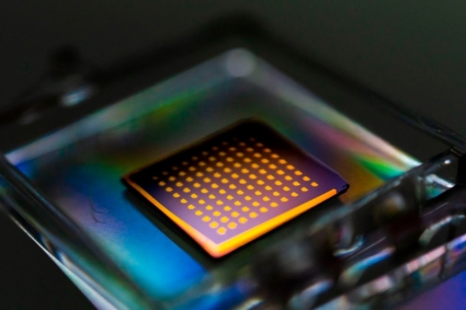 Researchers in MIT’s Department of Mechanical Engineering have developed a technique to harvest 2-inch diameter wafers of 2D material within just a few minutes. (Image: Peng Lin)
The method, which they illustrate in a paper reported in the journal Science, could lead to the possibility of commercializing electronic devices based on a range of 2D materials, according to Jeehwan Kim, an associate professor in the Department of Mechanical Engineering, who headed the research.
The paper’s co-first authors are Sang-hoon Bae, who worked on flexible device fabrication, and Jaewoo Shim, who was involved in the stacking of the 2D material monolayers. They are postdocs in Kim’s group.
The co-authors of the paper also included students and postdocs from within Kim’s group, as well as collaborators at Georgia Tech, the University of Texas, Yonsei University in South Korea, and the University of Virginia. Sang-Hoon Bae, Jaewoo Shim, Wei Kong, and Doyoon Lee in Kim’s research group equally contributed to this research.
We have shown that we can do monolayer-by-monolayer isolation of 2D materials at the wafer scale. Secondly, we have demonstrated a way to easily stack up these wafer-scale monolayers of 2D material.”
Jeehwan Kim, Senior Researcher
The MIT scientists primarily grew a thick stack of 2D material on top of a sapphire wafer. A 600-nanometer-thick nickel film was then applied to the top of the stack.
Since 2D materials stick a lot more strongly to nickel than to sapphire, lifting off this film allowed the scientists to separate the whole stack from the wafer.
Furthermore, the adhesion between the nickel and each layer of the 2D material is also greater than that between each of the layers themselves.
Consequently, when a second nickel film was then integrated to the bottom of the stack, the MIT scientists were able to lift off individual, single-atom thick monolayers of 2D material.
That is because peeling off the first nickel film creates cracks in the material that spread all the way to the bottom of the stack, Kim says.
Once the first monolayer collected by the nickel film has been moved to a substrate, the process can be carried out again for each layer.
We use very simple mechanics, and by using this controlled crack propagation concept we are able to isolate monolayer 2D material at the wafer scale."
Jeehwan Kim, Senior Researcher
The universal method can be used with a variety of different 2D materials, including tungsten disulfide, hexagonal boron nitride, and molybdenum disulfide.
Like this, it can be used to create various types of monolayer 2D materials, such as metals, semiconductors, and insulators, which can then be stacked together to develop the 2D heterostructures required for an electronic device.
The process is fast and economical, making it ideal for commercial operations, he adds.
The scientists have also shown the method by effectively fabricating arrays of field-effect transistors at the wafer scale, with a thickness of merely a few atoms.
“The work has a lot of potential to bring 2D materials and their heterostructures towards real-world applications,” says Philip Kim, a professor of physics at Harvard University, who was not involved in the work.
The researchers are, at present, planning to apply the method to create a range of electronic devices, such as flexible devices that can be worn on the skin and a nonvolatile memory array.
They are also keen on applying the method to build devices for use in the “internet of things,” Kim says.
All you need to do is grow these thick 2D materials, then isolate them in monolayers and stack them up. So it is extremely cheap — much cheaper than the existing semiconductor process.
This means it will bring laboratory-level 2D materials into manufacturing for commercialization.
That makes it perfect for IoT networks, because if you were to use conventional semiconductors for the sensing systems it would be expensive.”
Jeehwan Kim, Senior Researcher