Oct 15 2019
Integrated nanophotonics, which takes photons as information carriers, is widely used in optical communication, optical information processing, optical computing. Nanophotonic wavelength router, which can separate and steer different incident optical wavelengths into different output ports, is an essential component for photonic integration.
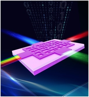
Recently, Prof. Cuicui Lu et al. in Beijing Institute of Technology have experimentally demonstrated ultrasmall broadband wavelength routers based on an intelligent algorithm. This work has been published in the Optica.
With the development of information technology, the requirements for the degree of integration are becoming higher and higher, including smaller size, broader band and lower loss of individual optical devices. However, in order to meet the above requirements, traditional design methods are challenged by using optical micro-cavities, photonic crystals, gratings, metal plasmonic structures, etc. The design process based on the traditional wavelength routers requires a large amount of computation resource and long time when optimizing the structure parameters, and the optimization process suffered serious limitations. An alternative solution is to design intelligent photonic devices by using intelligent optimization algorithms. In the work, Prof. Lu et al. design and experimentally demonstrate ultrasmall broadband wavelength routers for integration realized by using an intelligent algorithm that combines the genetic algorithm and the finite element method. The footprint of the wavelength router in the experiment is only 1.4 μm × 1.8 μm around the optical communication range. This is the smallest one ever demonstrated experimentally. Broad operation band, transmission up to 98%, and various output ports can be simultaneously achieved. It is convenient to realize various wavelength routers with different materials (both dielectric and metal), different configurations, different channels, different structure cell quantities or size. In addition, the average position error tolerance for each cell structure is about ±20 nm for all the wavelength routers designed by the intelligent algorithm, which satisfies the current nanofabrication technology. The device with planar configuration is very easy for fabrication and much suitable for the practical on-chip integration applications.
“We are doing further research on multi-functional cascaded nanoscale photonic devices by using intelligent algorithm and hope to realize an all-optical chip in future.” said Prof. Lu in Beijing Institute of Technology.
This work provides a new method for the universal design of nanophotonic wavelength routers, and will greatly promote the development of nanophotonic integrated devices, as well as the future applications in highly integrated photonic chips. It may change the general design methods for nanophotonic devices by human.
Source: http://english.bit.edu.cn/