Jan 21 2020
At the Center for Multidimensional Carbon Materials (CMCM) of the Institute for Basic Science (IBS), South Korea, scientists have fabricated and used single-crystal copper-nickel alloy foil substrates to grow large-area, single-crystal bi- and trilayer graphene films. The study was published in the Nature Nanotechnology journal.
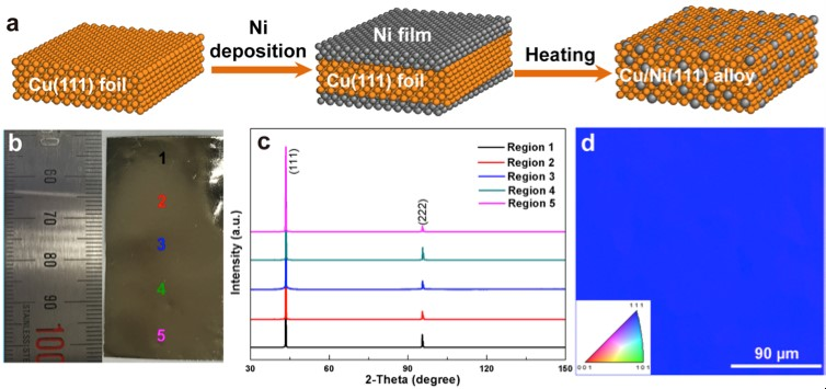 Preparation and characterization of Cu/Ni(111) foils. (a) Schematic of the preparation of the Cu/Ni(111) foils shows that Ni films are electroplated on both sides of a Cu(111) foil, which is followed by heating in a chemical vapor deposition chamber at 1050 °C for 5–7 hours to obtain the Cu/Ni(111) foil. By controlling the concentration of nickel (Ni), IBS researchers could obtain bilayer and trilayer graphene with the desired stacking order and large area. (b) A photograph of a piece of Cu/Ni(111) alloy foil (3 cm × 5 cm in size). (c) X-ray pattern taken from different regions across the whole sample (3 cm × 5 cm). (d) Electron backscatter diffraction map indicating the uniform (111) orientation of the prepared Cu foils. Image Credit: Institute for Basic Science.
The ability to grow large-area graphene films with accurately manipulated stacking orders and number of layers can pave the way for new opportunities in the fields of photonics and electronics. However, it has been highly difficult until now. This research demonstrated the first-ever production of bilayer and trilayer graphene sheets more than 1 cm in size. The layers were stacked in a particular way, that is, AB and ABA stacking.
This work provides materials for the fabrication of graphene devices with novel functions that have not yet been realized and might afford new photonic and optoelectronic and other properties.
Rodney S. Ruoff, Director, Center for Multidimensional Carbon Materials, Institute for Basic Science
Ruoff is the study’s lead author and Distinguished Professor at the Ulsan National Institute of Science and Technology (UNIST).
According to Professor Won Jong Yoo from Sungkyunkwan University, who is the co-author of the study, “This paves the way for the study of novel electrical transport properties of bilayer and trilayer graphene.”
For instance, recently, the same IBS research team and their collaborators published another article in Nature Nanotechnology, which demonstrates the transformation of AB-stacked bilayer graphene film, grown on copper/nickel (111) alloy foils (Cu/Ni(111) foils), into a diamond-like sheet, called diamane.
Less than one year ago, we produced fluorinated diamond monolayer, F-diamane, by fluorination of exactly the AB-stacked bilayer graphene films described in this new paper. Now the possibility of producing bilayer graphene of a larger size brings renewed excitement and shows how fast this field is developing.
Pavel V. Bakharev, Study Coauthor, Center for Multidimensional Carbon Materials, Institute for Basic Science
It is crucial to select the right substrate to ensure the precise growth of graphene. Foils made only of copper restrict bilayer graphene growth and promote uniform growth of monolayer graphene. Although multilayer graphene sheets can be obtained on nickel film, these are not even and could have small “patches” with varying thicknesses. Lastly, it is not ideal to use the commercially available foils made of both copper and nickel.
Hence, the IBS scientists developed “home-made” single-crystal Cu/Ni(111) foils with preferred features, further advancing a method proposed by the team in 2018 in the Science journal. By electroplating nickel films onto copper(111) foils, such that the copper and nickel interdiffuse upon heating, a new single-crystal foil including both elements at modifiable ratios is yielded.
Ruoff proposed this technique and oversaw Ming Huang’s evaluations of the perfect nickel concentrations to yield uniform graphene sheets with the intended number of layers.
Through chemical vapor deposition (CVD), bilayer and trilayer graphene sheets were grown on Cu/Ni(111) foils by the IBS team. Huang successfully synthesized AB-stacked bilayer graphene films measuring several square centimeters and encompassing 95% of the substrate area, as well as ABA-stacked trilayer graphene covering more than 60% of the substrate area.
This is the first time high-coverage ABA-stacked trilayer graphene has been grown over a large area and the highest quality achieved for AB-stacked bilayer graphene until now.
Apart from wide-scale microscopic and spectroscopic characterizations, the scientists also quantified the thermal conductivity and the electrical transport (bandgap tunability and carrier mobility) of the newly developed graphene.
The centimeter-scale bilayer graphene films exhibited optimal thermal conductivity, of up to ~2300 W/mK (analogous to exfoliated bilayer graphene flakes), and mechanical performance (stiffness of 3.31 gigapascals for the fracture strength, and 478 gigapascals for the Young’s modulus).
Then, the researchers analyzed the growth stacking mechanism and found that it conforms to what is called the “inverted wedding cake” sequence, as the bottom layers are positioned after the top one.
We showed with three independent methods that the 2nd layer for bilayer graphene, and the 2nd and 3rd layers of the trilayer sheet grow beneath a continuous top layer. These methods can be further used to study the structure and stacking sequence of other 2D thin film materials.
Ming Huang, Researcher, Center for Multidimensional Carbon Materials, Institute for Basic Science
According to Ruoff, these methods for producing and investigating large-scale ultrathin films could trigger worldwide interest in performing more experiments with single-crystal Cu/Ni alloy foils, and even in studying further the fabrication and use of other single-crystal alloy foils.
This study was conducted in partnership with UNIST and Sungkyunkwan University.
Source: https://www.ibs.re.kr/eng.do