Feb 7 2020
Scientists at Hokkaido University have developed a novel technique for creating nanosized semiconductors on a metal surface. The technique was described in the Nano Letters journal and could induce further studies into the development of nanosized light and energy emitters.
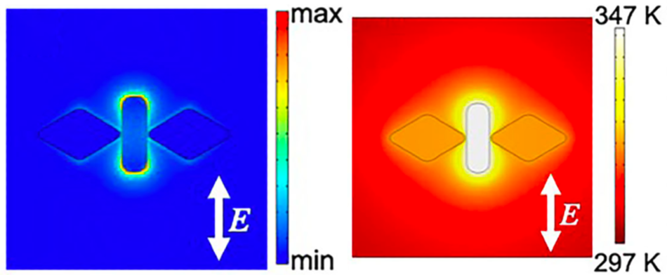 Calculated localized field (left) and temperature distribution (right) of the nano-butterfly structure. Image Credit: Fujiwara H., et al, Nano Letters. December 23, 2019.
Devised by Hokkaido University’s Research Institute for Electronic Science and Hokkai-Gakuen University, the technique involves producing localized heat on a gold nanoparticle inside a butterfly-shaped nanostructure. Due to the generated heat, hydrothermal synthesis occurs, making semiconducting zinc oxide to crystallize on the gold nanoparticle.
Researchers have been seeking methods to cautiously position nano-sized semiconductors on metallic particles to make use of them, for instance, in nano-lithography and nano-lasing. However, existing techniques are either highly inexpensive or lack precision.
The technique devised by the Japanese researchers resolves these problems.
Initially, the researchers performed simulations to ascertain the ideal conditions for achieving accurate control over the production of heat in nanostructures. A phenomenon named surface plasmon resonance was employed, which is a process that involves partly converting the light to heat in metallic materials.
The simulations demonstrated that when a butterfly-shaped nanostructure including two rhombus gold particles is placed on either side of a gold nanorod, optimal conditions can be achieved. The nanorod, or the body of the butterfly, in this system acts as a nanoheater that uses a particular polarized light.
When the light polarization is rotated by 90°, the rhombus particles (i.e., the butterfly’s wings) should act as an antenna to collect light at subwavelength spots in the semiconductor skin of the butterfly.
The research team tested this theory by fabricating the gold butterfly and positioning it in water within a glass chamber. To the chamber, a solution containing equal parts hexamethylene tetramine and zinc nitrate hexahydrate was added. Then, the chamber was sealed and positioned on a microscopic stage. Upon shining the laser light on the system within the chamber, as expected, the nanorod heated up and crystallization of semiconducting zinc oxide particles occurred along its surface.
This showed that the butterfly-shaped gold nano-antenna has the ability to accurately control at which place plasmon-assisted hydrothermal synthesis occurs. This facilitates the nanosized semiconductors to be formed in a localized manner.
Further research is expected to lead to the development of powerful nano-sized light sources, highly efficient photoelectric conversion devices, and photocatalysts. It could also lead to applications in semiconductor electronics and optical quantum information processing.
Keiji Sasaki, Researcher, Hokkaido University
Source: https://www.global.hokudai.ac.jp/