Researchers have published an article in The journal of Physical Chemistry Letters where the recent advances, as well as challenges associated with the development of 2D perovskite-based photodetectors, have been thoroughly assessed.
Study: Perovskite-Type 2D Materials for High-Performance Photodetectors. Image Credit: Niethammer Zoltan/Shutterstock.com
Introduction to Photodetectors
Photodetectors are light detectors that are often found in electronics products, medicinal imaging, and guidance systems.
Photodetectors are instruments that can transform light's photon power into electricity pulse.
Delicate and fast-response photodiodes are in great supply due to the constantly expanding need for improved picture detection and optic telecommunications.
Because of their tiny size, reliable diagnostic rate, and detection rate effectiveness, semiconductor photodetectors, also known as photodiodes, are the most popular types of photodiodes used in optical fiber communication.
Perovskite superconductors have advanced significantly in photonic applications in recent years, with the quality factor of perovskite photodiodes reaching levels equivalent to that of commercialized photodiodes.
Are Organic-Inorganic Hybrid Perovskites Beneficial?
Organic-inorganic hybrids perovskite materials have large photon outputs and are simple to implement, enabling light signal monitoring over a wide bandwidth spectrum in the UV-vis-IR domain.
In general, high-temperature manufacturing processes and short wavelengths attenuation coefficient limit conventional semiconductors, whereas poor carrier mobility limits nanoparticles and organic semiconductors.
Blended perovskites merge large light absorbance value, lengthy carrier mobility duration, lengthy transmission longevity, comparatively elevated sensitivity, and controllable energy band gap to profit from the benefits of both natural and inorganic semiconductor materials, resulting in substantial interest for use in high-performance photodiodes.
However, in large-scale photodetector uses, the long-term sustainability of hybrid perovskites remains a difficulty. Surprisingly, by lowering the structural dimension, the durability of hybrid perovskites may be successfully increased.
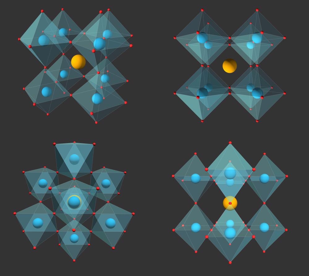
Two-Dimensional Perovskite-Based Materials
Perovskite-based 2D materials, influenced by nanoscale 2-D conjugated polymers, are thought to have substantial practical potential applications.
As a result, innovative highly conductive 2D materials with improved optoelectronic characteristics and wide direct band adjustability, in addition to existing semiconducting 2D materials, are in high demand.
Inheriting from 3D perovskite materials with exceptional inherent optoelectronic capabilities, 2D perovskite composites display equivalent photonic efficiency while exhibiting enhanced hydrophilicity, which is beneficial to the long-term sustainability of optoelectronics.
The research and development of 2D perovskite materials for next-generation photodetectors are still in their infancy.
When the width of single-crystalline 2D perovskites is reduced to slender or chemically thin levels, they can exhibit unusual optoelectronic efficiency, such as configurable assimilation by chemical configuration, augmented transmission detachment by impressive photo-sensing potential, and enhanced transmission retrieval by adaptable band designing.
Two-Dimensional Perovskite Photodetectors
In general, single crystals are required for 2D perovskite-based photodiodes.
Polycrystalline films are characterized by unpredictable crystallographic alignment, unanticipated transitions, and asymmetrical conduction characteristics, which result in undesired carrier segregation and accumulation.
As a result, single-crystalline 2D perovskite is projected to have remarkable photonic capabilities, owing to its lack of intergranular boundaries and reduced trap concentration.
One of the most essential factors in semiconductors is the visual bandgap.
A narrow-bandgap perovskite semiconductor is appropriate for infrared optical detection, whereas a wide-bandgap perovskite semiconductor is appropriate for ultraviolet optical detection.
Because directly producing semiconductors cannot always meet the demand for all bandgaps, band structure engineering is used to change the bandgap of perovskite semiconductors to achieve optimal performance.
Perovskite semiconductors' electrical parameters, in addition to their optical capabilities, are critical for photodiode purposes.
Widespread Applications
Large-scale silicon wafer fabrication exhibits several desirable and efficient functional characteristics for industrial optoelectronics, including spatial uniformity, exceptional optoelectronic qualities, and simplicity of integration.
Many 2D materials have been demonstrated to form wafer-scale monolayers on surfaces.
Microelectronic photonic technologies produce high-density semiconductors in electronic components, resulting in great responsiveness and portability.
Microelectronic photonic technologies generate high-density transistors in electronic parts, leading to high sensitivity and mobility.
Challenges and Limitations
Although these perovskite materials appear to be favorable, issues like a significant expense, physical stiffness, and high driving power remain significant barriers to real applications.
Solution-processed metal halide perovskite materials have exceptional optical efficiency and have been demonstrated to be appropriate for low-cost, substantial, adaptable, and interconnected photodetectors.
Controllable development of high-quality, large-area 2D perovskite nanocrystals is still a major difficulty.
It is critical to improve the development of 2D perovskite crystalline materials and subsequently construct optical devices to boost the advancement of sophisticated 2D perovskite-based photodiodes.
In short, 2D perovskite materials could significantly impact the future of optoelectronics, although much research is needed to overcome the field's challenges.
Reference
Li, Z. et al., (2022) Perovskite-Type 2D Materials for High-Performance Photodetectors. The Journal of Physical Chemistry Letters, Volume 13, pp. 1215-1225. Available at: https://pubs.acs.org/doi/10.1021/acs.jpclett.1c04225
Disclaimer: The views expressed here are those of the author expressed in their private capacity and do not necessarily represent the views of AZoM.com Limited T/A AZoNetwork the owner and operator of this website. This disclaimer forms part of the Terms and conditions of use of this website.