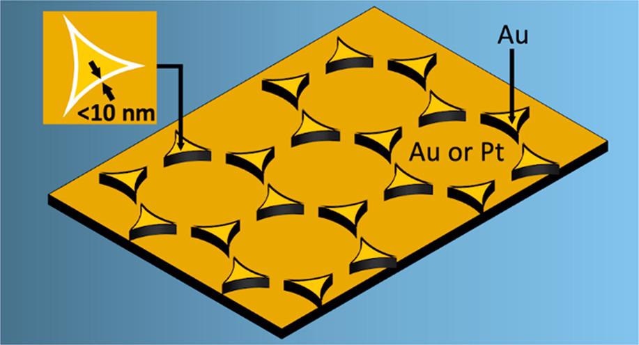
An article published recently in the journal ACS Nano describes a high-output approach for producing large-area matrices of triangular nanogaps. The nanogap matrices serve as highly effective SERS platforms.
Study: High-Throughput Fabrication of Triangular Nanogap Arrays for Surface-Enhanced Raman Spectroscopy. Image Credit: Luo, S., et al (2022)
An Introduction to Surface-Enhanced Raman Spectroscopy
Surface-enhanced Raman spectroscopy (SERS) is a popular approach for highly responsive detection in chemical research, biological monitoring, and catalytic processes. The metal platform is crucial in SERS detection, with nanometric features on the metallic surface functioning as "hot-spots" of a strong electromagnetic (EM) field. The Raman reaction of adsorbate species is significantly enhanced to species on a flat metallic sheet, enabling ultrasensitive detection.
![Fabrication procedure for triangular nanogap arrays: first, a monolayer of close-packed polystyrene nanospheres is drop-cast on a substrate and gently treated with an oxygen plasma to reduce surface asperities (a); second, a 50 nm layer of a first metal [M1] is deposited by e-beam deposition onto the nanosphere-coated substrate (b); third, the nanosphere template is removed by tape-stripping, leaving an array of triangular-shaped metal features on the substrate (c); fourth, the metal triangles are conformally coated with a molecular spacer formed from a self-assembled monolayer (SAM) or a self-assembled multilayer (d); fifth, the entire substrate is coated with a 30 nm layer of a second metal [M2] (e); and sixth, an adhesive film is applied to the upper surface of M2 and then stripped away, removing the parts of M2 that lie directly above the first metal. Finally, treatment with an oxygen plasma removes the spacer molecules, leaving M1 and M2 side by side on the substrate with triangular nanoscale gaps between them that are approximately equal in width to the length of the molecular spacer (f).](https://d1otjdv2bf0507.cloudfront.net/images/news/ImageForNews_38952_16494113719183271.jpg)
Figure 1. Fabrication procedure for triangular nanogap arrays: first, a monolayer of close-packed polystyrene nanospheres is drop-cast on a substrate and gently treated with an oxygen plasma to reduce surface asperities (a); second, a 50 nm layer of a first metal [M1] is deposited by e-beam deposition onto the nanosphere-coated substrate (b); third, the nanosphere template is removed by tape-stripping, leaving an array of triangular-shaped metal features on the substrate (c); fourth, the metal triangles are conformally coated with a molecular spacer formed from a self-assembled monolayer (SAM) or a self-assembled multilayer (d); fifth, the entire substrate is coated with a 30 nm layer of a second metal [M2] (e); and sixth, an adhesive film is applied to the upper surface of M2 and then stripped away, removing the parts of M2 that lie directly above the first metal. Finally, treatment with an oxygen plasma removes the spacer molecules, leaving M1 and M2 side by side on the substrate with triangular nanoscale gaps between them that are approximately equal in width to the length of the molecular spacer (f). © Luo, S., et al (2022)
Metal sheets with intentionally wrinkled or abraded surfaces have been employed in SERS technologies. Other materials include lithographically textured sheets with two-dimensional periodical matrices of nanostructured attributes, including holes, gaps, or stars that act as electromagnetic hotspots.
The recurrence of the manufactured hotspots offers spatially homogeneous amplification factors required for quantifiable SERS assessment, making matrix-based platforms especially appealing for SERS purposes. The difficulties of texturing periodical arrays across huge regions, on the other hand, have significantly restricted their applicability.
Existing Fabrication Methods and their Limitations
Etching organized metal matrices with SERS-active nanoscale patterns requires numerous nanoscale manufacturing techniques like electron-beam lithography (EBL), capillary force-assisted (CFA) lithography, extreme-UV lithography (EUVL), block copolymer lithography, focused-ion beam (FIB) milling. Breaking and cracking techniques are also utilized. Nonetheless, EBL, EUVL, and FIB techniques are too costly and time-consuming for producing dense nanostructured arrays across large regions. Although breaking and cracking techniques provide accessibility to very tiny gaps, the physical construction of the break junctions before the breakage phase is often performed by EBL or FIB milling; thus, they have output restrictions. Similarly, CFA and block copolymer lithographic techniques are limited to particular shapes, such as columns and concentric rings. Furthermore, since the manufactured nanostructures are made of a particular substance, it is not possible to utilize them to form binary nanoscale structures, which may give greater Raman responsiveness in some instances. As a result, there is a continuous demand for a quick, low-cost, and repeatable technique for imprinting nanostructures with gap sizes of ten nanometers or less.
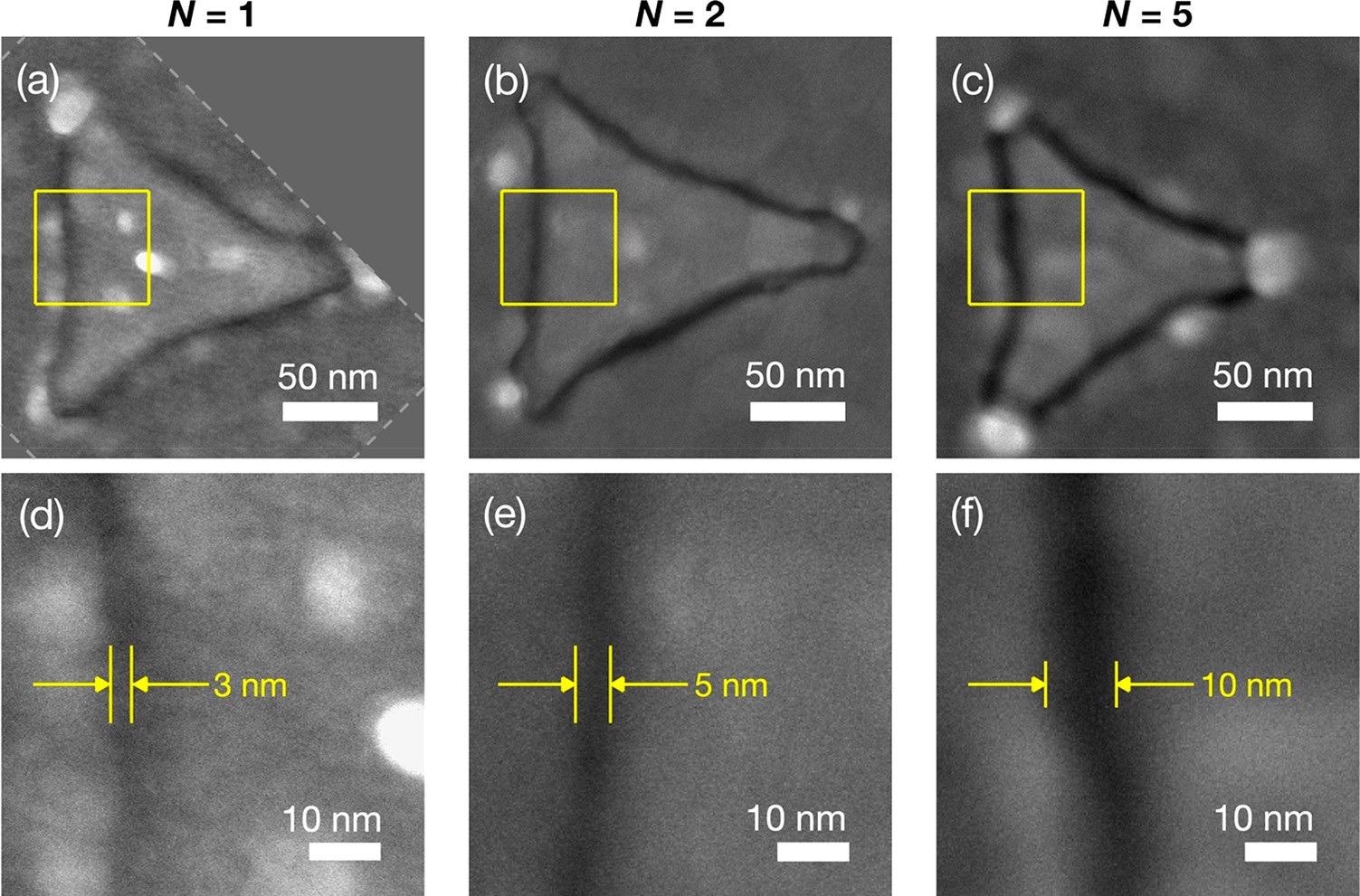
Figure 2. High-resolution SEM images of triangular Au/Au nanogaps. (a)–(c) SEM images showing a single triangular nanogap in an N = 1 (a), N = 2 (b), and N = 5 (c) TNG array. The yellow boxes enclose square regions of length 60 nm. The dotted white lines in (a) indicate the edge of the SEM image, which has been rotated to bring the left edge of the triangle into vertical alignment. (d)–(f) Magnified sections of the SEM images from (a)–(c), showing the yellow boxed regions. The approximate gap widths are 3, 5, and 10 nm for the N = 1 (d), N = 2 (e), and N = 5 (f) TNG arrays. © Luo, S., et al (2022)
Key Takeaways of the Study
The researchers proposed a straightforward, high-output approach for producing large-area packed matrices of triangular nanogaps (TNGs) that enables the gap size to be controlled from ten nanometers to less than three nanometers by employing a mix of colloidal nanosphere lithography, molecular self-arrangement, and physical peeling.
When exposed to 633 and 785-nanometer irradiations, the nanogap matrices serve as highly effective, spatially homogeneous platforms for SERS, with SERS action rising significantly as the gap size increases from three to ten nanometers.
EM models revealed that the intense SERS action was caused by the stimulation of the matrix's cumulative plasmon modes, which may lead to significant mean-squared field increases of more than 400 near the top of the gap.
The researchers managed to perform precise label-free identification of biomolecular adenine down to 100 pm utilizing a ten-nanometer triangular nanogap array. Moreover, they demonstrated that precise SERS detection is achievable on mixed-metal TNG matrices built on platinum and gold, raising the potential of accurate SERS assessment of reactive molecules on electrochemical and catalytic surfaces.
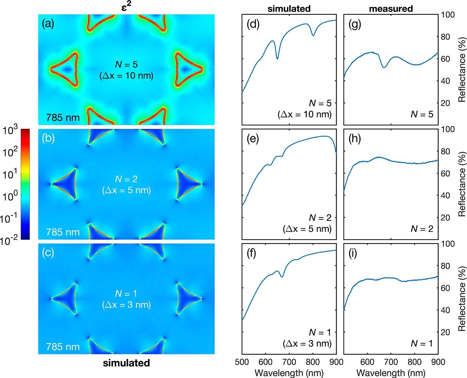
Figure 3. Simulated field-enhancement maps and simulated and experimental reflectance spectra for Au/Au TNG arrays. (a)–(c) Simulated plots showing the square of the field enhancement ε at a height z* = 30 nm above the glass substrate (i.e., coincident with the top surface of Au-2) for gap widths of 3 nm (N = 1), 5 nm (N = 2), and 10 nm (N = 5), assuming an unpolarized plane wave illumination at 785 nm. (d)–(f) Simulated reflectance spectra for gap widths of 3 nm (N = 1), 5 nm (N = 2), and 10 nm (N = 5), assuming an unpolarized, monochromatic plane-wave illumination in the range 500–900 nm. (g)–(i) Experimentally determined reflectance spectra for N = 1, N = 2, and N = 5 TNG arrays, using an unpolarized monochromatic, plane-wave illumination in the range 500–900 nm. © Luo, S., et al (2022)
Avenues for Future Work
Owing to their excellent SERS performance, the N = five triangular nanogap matrices could be tailored for SERS usage in some of the following ways. As the molecule ruler length was restricted to N = five owing to yielding difficulties at longer ruler lengths, further improvement of the gap size is a logical initial step. Another possibility is to substitute gold with silver, which has significantly higher SERS performance; however, this would necessitate replacing the oxygen plasma treatment required to eliminate the molecular spacer with a procedure that does not lead to the etching of silver.
Simulations show that the pitch seems to have a significant impact on the plasmonic behavior of the matrices and optimizing the pitch (by adjusting the nanosphere radius) is anticipated to boost SERS performance even more. Additional geometric parameters, such as how thick the metallic films are, and the step-height between the two different metals, are also expected to impact SERS performance.
Reference
Luo, S., Mancini, A., Wang, F., Liu, J., Maier, S. A., & de Mello, J. C. (2022). High-Throughput Fabrication of Triangular Nanogap Arrays for Surface-Enhanced Raman Spectroscopy. ACS Nano. Available at: https://doi.org/10.1021/acsnano.1c09930
Disclaimer: The views expressed here are those of the author expressed in their private capacity and do not necessarily represent the views of AZoM.com Limited T/A AZoNetwork the owner and operator of this website. This disclaimer forms part of the Terms and conditions of use of this website.