A professor at RUDN has proposed a method for fabricating porous silicon nanostructures that are confined to a certain area. As a result, it will be easier to construct silicon substrates with neurons and other biological components, such as when making neuroprocessors. The results were published in Processes.
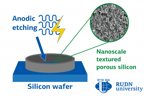
Image Credit: RUDN University.
About one-millionth of a millimeter-wide silicon nanoparticle was used. It contains so many holes that one gram of matter has a surface area of up to 1000 m2. For instance, such an area may be utilized to turn live neurons into “microprocessors.” To do this, one must understand how to create such porous nanostructures in the intended isolated zone of the silicon substrate.
An approach to produce nanoporous silicon locally was put out by the associate professor of RUDN. The technique will aid in the “settling” of biological components such as neurons on the nanostructure.
The main characteristic of nanostructured porous silicon which prevails in most cases of practical applications is a very significant specific surface area. Therefore, the formation of various membrane and electrode structures based on silicon is of considerable interest.
Ekaterina Gosteva, Ph.D., Associate Professor, Department of Nanotechnology and Microsystem Engineering, Academy of Engineering, RUDN University
In a proposal, researchers from RUDN, MISIS, and the Institute of Microelectronics Technology and High Purity Materials suggested making silicon nanostructures using the anode etching techniques. The electrolytic dissolution of the initial material from the substrate is the key step in the process. The required structure is then left on the plate.
The scientists made use of a tiny silicon wafer with a thin (0.2–0.3 mm) oxide coating covering one side. It was then covered with a ring made of the “reinforced” rubber durite. It produced a barrier around the region where nanoporous silicon was made. As a result, the plate outside the ring is unaffected by electric etching.
Additionally, the nanopores are generated uniformly inside the ring itself. The only exception is a layer close to the ring’s edge that is one micrometer thick. There, the pores look like slits and become elongated.
Our results suggest that it is practical to localize the porous region on the silicon wafers without any noticeable effect on their structure outside the porous region. The porous structure is fairly uniform throughout the area. The proposed scheme makes it possible to conduct experiments with biological objects—for example, stem cells, neurons, and other objects—in a locally formed porous structure.
Ekaterina Gosteva, Ph.D., Associate Professor, Department of Nanotechnology and Microsystem Engineering, Academy of Engineering, RUDN University
Journal Reference:
Starkov, V. V. E., et al. (2022) Nanoporous Layers and the Peculiarities of Their Local Formation on a Silicon Wafer. Processes. doi.org/10.3390/pr10010163.
Source: https://eng.rudn.ru/