A significant advancement in the transfer of two-dimensional crystals has been accomplished by researchers at the University of Manchester, which could advance their commercialization in next-generation electronics. Published in Nature Electronics, the new method utilizes a completely inorganic stamp to manufacture uniform and anatomically clean 2D material stacks like never before
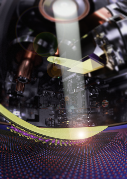
Image Credit: The University of Manchester
Under the direction of Professor Roman Gorbachev of the National Graphene Institute, the group conducted their investigation in an ultra-high vacuum environment, using the technique to “pick and place” 2D crystals into van der Waals heterostructures consisting of up to 8 separate layers.
This breakthrough led to atomically clean interfaces across large regions, which is a major improvement over current methods and a necessary step toward the commercialization of electrical devices based on 2D materials.
Furthermore, strain inhomogeneity in constructed stacks was successfully minimized by the new stamp design’s rigidity. When comparing the ‘twisted’ interfaces to the state-of-the-art assemblies that are already in use, the researchers saw a notable drop in local variance that is many orders of magnitude smaller.
The ability to precisely stack distinct 2D materials in predetermined sequences might lead to the atomic-level engineering of designer crystals with unique hybrid features. Although several methods for transferring single layers have been devised, nearly all of them rely on organic polymer membranes or stamps to provide mechanical support as the layers move from their originating substrates to the target ones.
Unfortunately, even in carefully maintained cleanroom conditions, this dependence on organic materials eventually introduces surface contamination of 2D materials.
Surface impurities caught in between layers of 2D materials frequently spontaneously split into isolated bubbles that are separated by atomically clean regions.
This segregation has allowed us to explore the unique properties of atomically perfect stacks. However, the clean areas between contaminant bubbles are generally confined to tens of micrometers for simple stacks, with even smaller areas for more complex structures involving additional layers and interfaces.
Roman Gorbachev, Professor, National Graphene Institute, The University of Manchester
He added, “This ubiquitous transfer-induced contamination, along with the variable strain introduced during the transfer process, has been the primary obstacle hindering the development of industrially viable electronic components based on 2D materials.”
When conventional methods use polymeric supports, it impedes attempts to remove ambient and pre-existing pollutants and serves as a source of nanoscale contamination. For example, at high temperatures, adsorbed contaminants can become completely desorbed or become more mobile, while polymers usually cannot tolerate temperatures higher than a few hundred degrees. Furthermore, polymers tend to outgas under vacuum settings and are incompatible with a wide range of liquid cleaning solutions.
To overcome these limitations, we devised an alternative hybrid stamp, comprising a flexible silicon nitride membrane for mechanical support and an ultrathin metal layer as a sticky ‘glue’ for picking up the 2D crystals. Using the metal layer, we can carefully pick up a single 2D material and then sequentially ‘stamp’ its atomically flat lower surface onto additional crystals. The van der Waals forces at this perfect interface cause adherence of these crystals, enabling us to construct flawless stacks of up to 8 layers.
Dr. Nick Clark, Study Second Author, The University of Manchester
After successfully proving the technology using minuscule flakes mechanically exfoliated off crystals using the ‘sticky tape’ method, the researchers scaled up the ultraclean transfer process to handle larger materials produced from the gas phase, achieving clean transfer of mm-scale regions. Working with these ‘grown’ 2D materials is critical to their scalability and possible uses in next-generation electronic devices.
Recognizing the importance of the discovery, the University of Manchester has submitted a pending patent application to protect both the method and the equipment. The research team is now keen to work with industry partners to evaluate the efficacy of this technology for wafer-scale transfer of 2D films from growing substrates.
They are looking for expressions of interest from equipment manufacturers, semiconductor foundries, and electronic device makers that have 2D materials in their product roadmap.
Journal Reference:
Wang, W, et. al. (2023) Clean assembly of van der Waals heterostructures using silicon nitride membranes. Nature Electronics. doi:10.1038/s41928-023-01075-y.
Source: https://www.manchester.ac.uk/