In a new study published in ACS Nano, researchers from the Harvard John A. Paulson School of Engineering and Applied Sciences (SEAS) have unveiled a 10-centimeter-diameter glass metalens capable of taking high-resolution images of celestial bodies like the sun, moon, and distant nebulae.
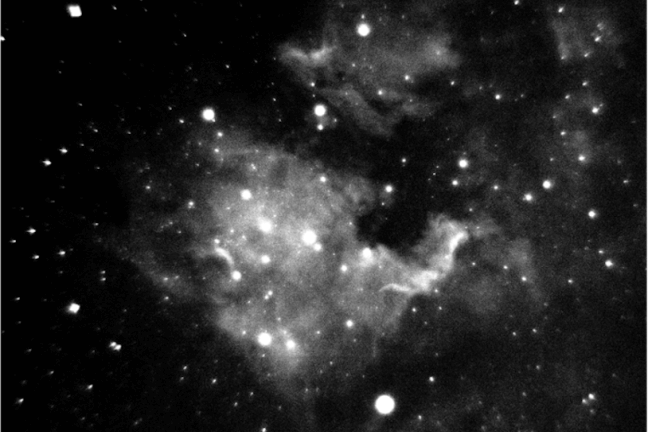 Image of the North America Nebula, in the constellation Cygnus, taken by the metalens on the roof of the Science Center in Cambridge. Image Credit: Capasso Lab/Harvard SEAS
This breakthrough, marking the first large-scale, visible-wavelength metalens crafted entirely from glass, can be mass-produced with traditional CMOS manufacturing techniques.
The ability to accurately control the size of tens of billions of nanopillars over an unprecedentedly large flat lens using state-of-the-art semiconductor foundry processes is a nanofabrication feat that opens exciting new opportunities for space science and technology.
Federico Capasso, Study Senior Author and Robert L. Wallace Professor of Applied Physics, Harvard John A. Paulson School of Engineering and Applied Sciences (SEAS), Harvard University
Most flat metalenses are around the size of a piece of glitter and concentrate light using millions of pillar-like nanostructures. By using a method known as deep-ultraviolet (DUV) projection lithography, Capasso and his colleagues created a centimeter-scale metalens in 2019.
This method eliminates the laborious writing and deposition processes necessary for earlier metalenses and projects a nanostructure pattern that can be directly etched into the glass wafer.
Fine lines and shapes are often patterned in silicon chips for computers and cellphones using DUV projection lithography. As a current postdoctoral fellow in Capasso’s lab and a graduate student at SEAS, Joon-Suh Park showed that the technology could produce the metalenses at scale and enlarge them for usage in virtual and augmented reality applications.
However, there was an engineering challenge to make the metalens significantly larger for astronomy and free-space optical communications applications.
There is a major limitation with the lithography tool because these tools are used to make computer chips, so chip size is restricted to no more than 20 to 30 millimeters. In order to make a 100-millimeter diameter lens, we needed to find a way around this limitation.
Joon-Suh Park, Postdoctoral Fellow, Harvard John A. Paulson School of Engineering and Applied Sciences (SEAS), Harvard University
Park and colleagues created a method for employing the DUV projection lithography tool to piece together several nanopillar designs. In just a few minutes, the researchers demonstrated that DUV projection lithography could pattern 18.7 billion planned nanostructures onto a 10-centimeter circular region by splitting the lens into twenty-five parts and only using the 7 sections of a quadrant that took rotational symmetry into account.
The group also created a vertical glass etching method that enables the etching of smooth sidewall and high aspect ratio nanopillars into glass.
Using the same DUV projection lithography, one could produce large-diameter, aberration-correcting meta-optics or even larger lenses on larger glass diameter wafers as the corresponding CMOS foundry tools become increasingly available in the industry.
Soon Wei Daniel Lim, Study Co-First Author and Postdoctoral Fellow, Harvard John A. Paulson School of Engineering and Applied Sciences (SEAS), Harvard University
Lim was the main contributor to the comprehensive simulation and characterization of all potential fabrication faults that can occur during mass-manufacturing procedures and how they might affect metalenses’ optical performance.
The researchers then addressed potential production issues before showcasing the metalens’ ability to image astronomical objects.
Park and the group went to the roof of Harvard’s Science Center and mounted the metalens on a tripod equipped with a color filter and a camera sensor. There, they captured images of the Sun, Moon, and North America Nebula, a faint nebula located 2,590 light-years away in the constellation Cygnus.
Arman Amirzhan, a graduate student in the Capasso Lab and co-author of the study, added, “We were able to get very detailed images of the Sun, the moon and the nebula that are comparable to images taken by conventional lenses.”
The researchers were able to capture the same sunspot cluster as a NASA image from that same day, using only the metalens.
The group also showed that the lens would not suffer any damage or loss of optical function from exposure to extremely high or low temperatures as well as the strong vibrations that would be experienced during a space launch.
The lens might possibly be utilized for directed energy transmission and long-distance telecommunications due to its size and monolithic glass composition.
Hyukmo Kang, Karlene Karrfalt, Daewook Kim, Joel Leger, Augustine Urbas, Marcus Ossiander, and Zhaoyi Li are co-authors of the study. It was funded by the Air Force Office of Scientific Research under Award No. FA9550-22-1-0312 and the Defense Advanced Research Projects Agency (DARPA) under Grant No. HR00111810001.
Journal Reference:
Park, J.-S., et. al. (2023) All-Glass 100 mm Diameter Visible Metalens for Imaging the Cosmos. ACS Nano. doi:10.1021/acsnano.3c09462.
Source: https://seas.harvard.edu/