The introduction of the UVISEL VUV phase modulated spectroscopic ellipsometer from HORIBA Scientific extends the performance capabilities of the UVISEL series down to 140 nm. This energy range is becoming increasingly important for the characterisation of extremely thin films used in nanoscale devices with nanoelectronic, nanophotonic, nanobiosensor and nanorobotic applications.
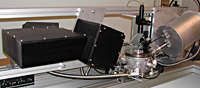 UVISEL VUV ellipsometer
The UVISEL VUV ellipsometer provides the best combination of superior VUV performance and experimental flexibility to determine thin film thickness and optical constants across the wavelength range 140 to 826 nm. Features of the UVISEL VUV include:
- Wide spectral range at very high speed
- Advanced design for high performance in the VUV
- Direct sample access and fast loading
- Phase modulation technology for high accuracy and precision measurement
- Excellent signal to noise and signal to background ratio
To be able to cover this wide range the instrument must be air / oxygen free, and it is this requirements that can reduce sample throughput for some instruments owing to ingress of air and its removal when the sample is mounted and dismounted from the instruments.
To minimize this affect the UVISEL VUV is configured as three separate compartments; the lamp + polarizer, the sample chamber, and the photoelastic modulator + monochromator + photomultiplier detection system. The sample compartment has separate access and is equipped with its own isolated purge system.
This design provides high flexibility and versatility for sample handling, and enables high sample throughput.
The UVISEL VUV is controlled by the Deltapsi2 software platform, and is ideal for VUV thin film applications for demanding research and industrial quality control.
VUV Thin Film Applications
VUV spectroscopic ellipsometry applications range from the measurements of the optical constants and optical bandgap of materials absorbing far in the UV such as high k materials, organic materials, stepper optics, photoresists.
VUV spectroscopic ellipsometry provides increased precision for thickness measurement of very thin layers and interfaces. This is especially useful for nanoscale applications where the characterization of a native oxide, a rough over layer or an interface affects the efficiency of the final device.