Feb 18 2009
Applied Microengineering Ltd (AML), world leaders in wafer bonding machines and bonding services, has announced the launch of its multi-million pound BONDCENTRE and new advanced bonded substrate business. The state-of-the-art facility, now complete, is situated on the UK's premiere science park in Harwell, Oxfordshire.
The new BONDCENTRE, a UK centre of excellence, enables AML to make its 20 years experience in wafer bonding available to start-up's, large corporate and government R&D labs, manufacturing businesses and academic institutions. It delivers these national and international organisations the ability to speed up technology, process and product development, as well as providing a smooth transfer of technology to volume production for improved time to market.
CEO of AML, Rob Santilli explains: “BONDCENTRE services are increasingly in demand for innovative new market applications, including MEMS, microelectronics, life sciences, optics, compound semiconductors, wafer level packaging, 3D integration and advanced bonded substrates.”
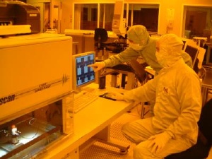
Equipped with AML's unique Aligned Wafer Bonder machines and staffed by the UK's most talented experts in commercial wafer bonding techniques, the BONDCENTRE is currently the only commercial facility in the world to provide wafer bonding and associated services for 2", 3", 4", 6" and 8" wafers, in a class 10 clean room environment. Outsourcing to BONDCENTRE makes economic sense, reducing timescales and negating investment in equipment, facilities and know-how.
Completing the launch of the BONDCENTRE is AML's new advanced bonded substrate business initially available for substrates including Silicon-Glass, Silicon<100>-Silicon<111> and Silicon-Quartz. Wafers can be pre-machined (holes and channels) and supplied with conducting via arrays before bonding, for use in wafer level packaging and 3D integration.
Santilli adds: “A core strength of the BONDCENTRE is the ability not only to offer bonding but also related services such as powder blasting, screen printing, CMP, electroplating metrology and inspection all under one roof. In the past, our customers may have had wafers CMP'd in the USA, drilled in Japan, screen printed with glass frit in Germany and bonded in the UK. At BONDCENTRE we can do this all in one location ensuring their product innovations can be brought to market faster.”