FA engineers are expected to produce accurate results. Thus, there is no room for error when it comes to the data provided by instruments. Due to its data precision, the Park NX20 is recognized as the most accurate large-sample AFM globally, especially in the semiconductor and hard disk industries.

Image Credit: ShutterStock/3dartists
More Powerful Failure Analysis Solutions
The Park NX20 is equipped with special features that help uncover the cause of device malfunctions and develop more creative solutions.
Its high accuracy provides detailed data, allowing focused work, and its True Non-Contact™ scanning mode maintains the sharpness of tips for longer, reducing the need and costs associated with tip replacement.
Easy to Use, Even for Entry Level Engineers
The Park NX20 has one of the simplest designs and automated interfaces in the industry. This saves time and effort in using the tool and guiding junior engineers.
This way, more attention can be given to addressing complex issues and providing timely failure analysis to customers.
Accurate AFM Solutions for FA and Research Laboratories
Sidewall Measurements for 3D Structure Study
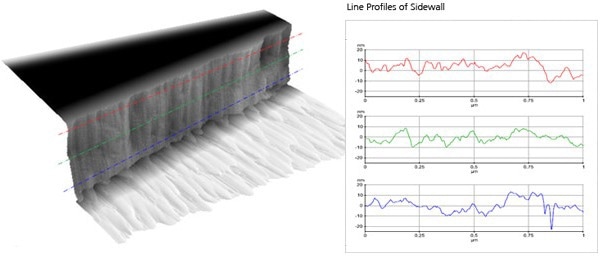
Image Credit: Park Systems
The NX20's innovative design allows the detection of sample sidewalls and surfaces, enabling angle measurements. This flexibility supports innovative research and deeper insights.
Surface Roughness Measurements for Media and Substrates
The assessment of surface roughness is a crucial application where the Park NX20 excels, ensuring accurate failure analysis and quality assurance.
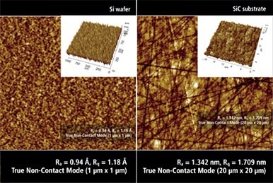
Image Credit: Park Systems
High-Resolution Electrical Scan Mode
QuickStep SCM
The Fastest Scanning Capacitance Microscopy
PinPoint AFM
The Frictionless Conductive AFM
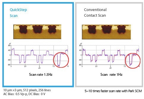
Image Credit: Park Systems
Accurate and Reproducible Measurements for Better Productivity
Tip Lifetime Performance Data on Polished Silicon Wafer: 15,000 Scans @ 10 Hz Using 1 Tip
Video Credit: Park Systems
Reproduce the Best AFM Measurement
The True Non-Contact Mode preserves tip sharpness even after capturing 200 images of the abrasive CrN, known as the tip check sample. CrN has a highly abrasive surface that could quickly wear out a standard tip.
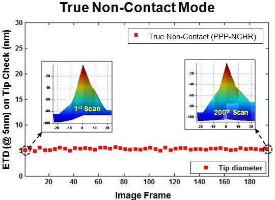
Image Credit: Park Systems
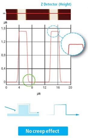
Accurate AFM Topography with Low Noise Z Detector
True Sample Topography™ Without Piezo Creep Error
Park Systems' AFMs have efficient low-noise Z detectors that are among the best in their field. These detectors have a noise level of 0.02 nm over a wide range, which results in accurate sample topography without edge overshoot or the need for frequent calibration. This is one way that Park AFM saves time and provides better data.
- The low-noise Z detector signal is used for topography.
- The Z detector has low noise, measuring 0.02 nm over a wide range.
- There is no edge overshoot at the leading and trailing edges.
- Calibration is only required once at the factory.
| Park NX AFM |
Conventional AFM |
 |
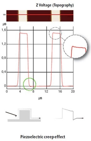 |
Image Credit: Park Systems
QuickStep SCM Mode
High Throughput QuickStep Scan
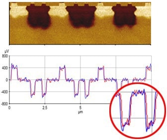
By using QuickStep scanning, the speed of SCM measurement is increased significantly — up to ten times that of standard SCM scans. However, this speed boost does not compromise signal sensitivity, spatial resolution, or data accuracy.
In QuickStep scanning, the XY scanner stops at each pixel to record data, making quick transitions between pixels.
- Ten times faster than a conventional SCM scan
- No compromise of signal sensitivity, spatial resolution, or data accuracy
| QuickStep Scan |
|
Conventional Scan |
Rather than continuous movements, the XY scanner stop at each data acquisition point. |
|
 |
Scan rate 1.5 Hz |
|
Scan rate 1 Hz |
Scan size: 10 µm × 3 µm, AC Bias: 0.5 Vp-v, DC Bias: 0 V. Image Credit: Park Systems
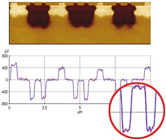
Accurate Dopant Profiling by Park SCM
In semiconductor manufacturing, accurately characterizing the dopant profile is important for identifying failures and making design improvements. Scanning capacitance microscopy (SCM) is unique in its ability to quantitatively measure 2D dopant profiles for device characterization.
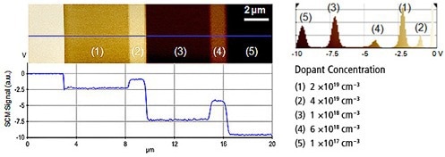
Image Credit: Park Systems
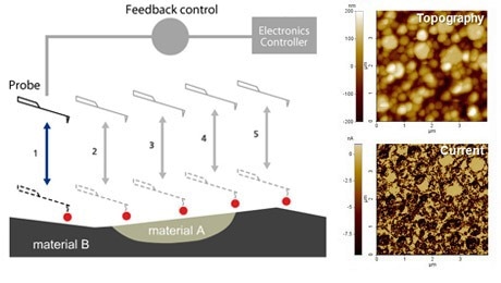
PinPoint Conductive AFM Mode
PinPoint Conductive AFM was created for precise electric contact between the tip and the sample. The XY scanner stops during electric current measurement, which can be controlled by the user. PinPoint Conductive AFM offers higher spatial resolution without lateral force and optimized current measurement on different sample surfaces.
| PinPoint Mode |
|
Contact |
Tapping |
 |
|
Sample: ZnO nano-rods, -3 V sample bias |
Image Credit: Park Systems
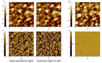
The comparison of conductive AFM images of ZnO nanorods shows that the conventional contact conductive AFM may have a higher current measurement than tapping conductive AFM, but its resolution is compromised as the tip wears out in contact mode topography.
The new PinPoint conductive AFM combines higher spatial resolution with optimized current measurement.
High-Bandwidth, Low-Noise Conductive AFM
Conductive AFM is crucial for device research, especially when it comes to failure analysis in industry. Park's conductive AFM stands out with competitive specifications, including the industry's lowest current noise level and a wide gain range.
- The lowest current noise level in the industry (0.1 pA)
- Maximum current in the industry (10 μA)
- Largest gain selection covers seven orders of magnitude (103 ~109)
Park NX20 Advanced SPM Modes (*Optionally Available)
Standard Imaging
- True Non-Contact™ Mode
- PinPoint™ AFM
- Basic Contact AFM
- Lateral Force Microscopy (LFM)
- Phase Imaging
- Intermittent (tapping) AFM
Electrical Characterization
- Scanning Capacitance Microscopy (SCM)*
- Conductive AFM*
- Electrostatic Force Microscopy (EFM)
- Piezoresponse Force Microscopy (PFM)
- Kelvin Probe Force Microscopy (KPFM)
General Characterization
- Magnetic Force Microscopy (MFM)*
- Scanning Thermal Microscopy (SThM)*
- Scanning Tunneling Microscopy (STM)*
- Force Modulation Microscopy (FMM)
- Nanoindentation*
- Nanolithography*
- Nanomanipulation*
Park NX20 Specification
Scanner
Z Scanner
- Guided high-force flexure scanner
- Scan range: 15 µm (optional 30 µm)
- Height noise level: 30 pm
- 0.5 kHz bandwidth, rms (typical)
XY Scanner
- Single module flexure XY-scanner with dual servo closed-loop control
- Scan range: 100 µm × 100 µm (optional 50 µm × 50 µm)
Stage
- Z stage range: 25 mm (Motorized)
- Focus travel range: 15 mm (Motorized)
- XY stage travel range: 150 mm x 150 mm (Motorized)
Sample Mount
- Sample size: Open space up to 150 mm x 150 mm, thickness up to 20 mm (Optionally, up to 200 mm x 200 mm)
- Sample weight: < 500 g
Optics
- 10x (0.23 NA) ultra-long working distance lens (1 µm resolution)
- Direct on-axis vision of sample surface and cantilever
- Field-of-view: 840 × 630 µm (with 10× objective lens)
- CCD: 1 M pixel, 5 M pixel (optional)
Software
SmartScan™
- Dedicated system control and data acquisition software
- Adjusting feedback parameters in real-time
- Script-level control through external programs (optional)
XEI
AFM data analysis software
Electronics
Integrated Functions
- 4 channels of flexible digital lock-in amplifier
- Digital Q control
Signal Processing
- ADC: 18 channels 4 high-speed ADC channels 24-bit ADCs for X, Y, and Z scanner position sensor
- DAC: 17 channels 2 high-speed DAC channels 20-bit DACs for X, Y, and Z scanner positioning
- Maximum data size: 4096 x 4096 pixels
External Signal Access
- 20 embedded signal input/output ports
- 5 TTL outputs: EOF, EOL, EOP, Modulation, and AC bias
AFM Modes (*Optionally Available)
Standard Imaging
- True Non-Contact AFM
- PinPoint™ AFM
- Basic Contact AFM
- Lateral Force Microscopy (LFM)
- Phase Imaging
- Tapping AFM
Force Measurement
- Force Distance (F/d) Spectroscopy
- Force Volume Imaging
Dielectric/Piezoelectric Properties
- Electric Force Microscopy (EFM)
- Dynamic Contact EFM (EFM-DC)
- Piezoresponse Force Microscopy (PFM)
- PFM with High Voltage*
Mechanical Properties
- Force Modulation Microscopy (FMM)
- Nanoindentation*
- Nanolithography*
- Nanolithography with High Voltage*
- Nanomanipulation*
Magnetic Properties*
- Magnetic Force Microscopy (MFM)
- Tunable Magnetic Field MFM
Electrical Properties
- Conductive AFM (C-AFM) *
- IV Spectroscopy*
- Kelvin Probe Force Microscopy (KPFM)
- Scanning Capacitance Microscopy (SCM)*
- Scanning Spreading-Resistance Microscopy (SSRM)*
- Scanning Tunneling Microscopy (STM)*
- Photo Current Mapping (PCM)*
Chemical Properties*
- Chemical Force Microscopy with Functionalized Tip
- Electrochemical Microscopy (EC-AFM)
AFM Options
The NX20 includes Park's automation control software, which performs AFM measurements on samples according to set procedures.
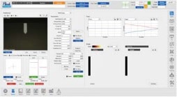
Image Credit: Park Systems
It accurately gathers data, carries out pattern recognition, and conducts analysis using its built-in Cognex board and optics module. Results are exported with little user effort, providing more time for research.
The NX20's design allows users to identify sample sidewalls and surfaces, making angle measurements possible. This flexibility helps researchers conduct advanced studies and gain important insights.
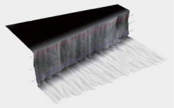
Image Credit: Park Systems
Active Temperature Controlled Acoustic Enclosure
The Park NX20 achieves temperature equilibrium rapidly through its innovative control design. Additionally, it includes active vibration isolation technology.
Encoders for Motorized Stage
- The encoded XY stage travels in 1 µm resolution with 2 µm repeatability
- The encoded Z stage travels in 0.1 µm resolution with 1 µm repeatability
Sample Plates
- Dedicated small sample holder for electrical measurements
- Vacuum grooves to hold wafers
Temperature Control
- Temperature Controlled Stage 1: -25 °C to +170 °C
- Temperature Controlled Stage 2: Ambient to +250 °C
- Temperature Controlled Stage 3: Ambient to +600 °C
Dimensions in mm
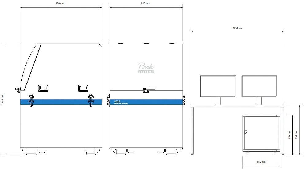
Image Credit: Park Systems
This information has been sourced, reviewed and adapted from materials provided by Park Systems.
For more information on this source, please visit Park Systems.