Sponsored by Park SystemsReviewed by Olivia FrostJun 12 2025
Comprehending failure modes, mechanisms, and root causes is vital in the production of semiconductors and electronic devices. Pinpointing the primary cause of failure is key to preventing its recurrence and ultimately improving product quality, reducing costs, and boosting customer satisfaction.
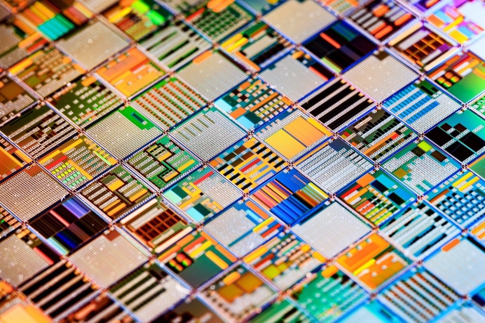
Image Credit: Andrei Armiagov/Shutterstock.com
In semiconductor manufacturing, failure analysis involves the inspection and characterization of localized defects on bare wafers, quality assessment across multi-stage processes, and evaluation of the function and performance of completed devices.
As electronic components continue to shrink, failure analysis becomes increasingly complex due to the reduced dimensions and intricate structures of micro- and nano-scale devices. This growing complexity underscores the need for a powerful yet user-friendly analysis tool capable of inspecting, isolating, and characterizing defects with precision.
This article explores key aspects of failure analysis methodologies in semiconductor and electronic device manufacturing, with a particular focus on the use of Atomic Force Microscopy (AFM) as an effective and versatile tool for advanced defect analysis.
 Download your copy now to read on!
This information has been sourced, reviewed and adapted from materials provided by Park Systems.
For more information on this source, please visit Park Systems.