A new review in Nanoenergy Advances argues that graphene-family materials could help tackle one of artificial intelligence’s most pressing problems: energy use.
 Study: Graphene-Based Memristive and Photomemristive Nanosensors for Energy-Efficient Information Processing. Image Credit: AntiAthom/Shutterstock.com
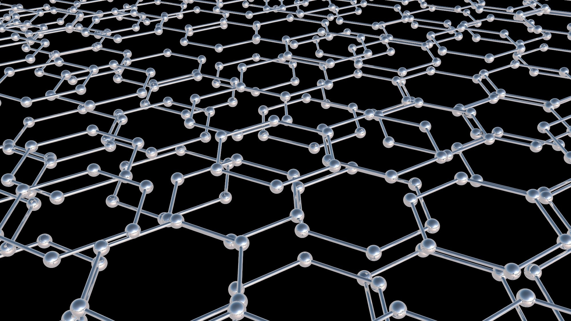
In the paper, Panin outlines how low-dimensional carbon-based materials, including graphene, graphene oxide, and diamane, are enabling energy-efficient processing of electrical and optical signals across a wide spectral range, from ultraviolet to infrared.
The work surveys how these materials support memristive and photomemristive nanosensors that merge sensing, memory, and computation into compact, low-power systems.
Saving this for later? Download a PDF here.
A large part of the current AI conversation is its energy use. Tesla’s DOJO processor, for example, performs 1.1 EFLOPs (∼10¹8 operations per second) while consuming 45 MW of power - comparable to a small power plant.
Such figures highlight the cost of shuttling vast amounts of data between sensors, memory, and processors in conventional von Neumann architectures.
Memristors may offer a different route. As non-volatile resistive switching devices, often described as the fourth fundamental circuit element, they store information in their resistance states.
Crucially, they allow logic and memory to coexist in the same physical structure. That opens the door to in-memory and even in-sensor computing, where data can be processed at or near the point of detection rather than transferred across energy-intensive architectures.
How Graphene Controls Resistance At Low Power
The review details how memristive states in graphene/graphene oxide and bigraphene/diamane nanostructures can be tuned at bias voltages below 1 V. Switching is governed by changes in sp3-sp2 hybridization of carbon atoms, along with interface-mediated redox processes that allow multilevel, low-energy control of resistive states.
Several fabrication strategies are discussed.
“Direct electron-beam writing” enables the formation of reduced graphene oxide (EB-rGO)/graphene oxide heterostructures with well-controlled resistive switching.
Laser lithography is another option: Graphene oxide memristors fabricated at laser powers between 65 and 75 mW exhibit the highest resistance ratios. A lateral Pt/GO/rGO device produced via direct laser writing demonstrated ultralow power consumption of 200 nW while displaying synaptic-like behavior.
Graphene oxide memristors have also been integrated into logic-in-memory circuits using MAGIC architecture. These devices implement Boolean operations (NOT, NOR, OR, AND, NAND) and exhibit unipolar resistive switching with on/off ratios exceeding 102. Their operation is linked to the reversible formation and rupture of nickel filaments.
Unlike conventional CMOS logic, such non-volatile circuits can achieve zero static power consumption in standby mode.
Memristors To Photomemristive Vision
The concept extends beyond this electrical switching ability.
A MoS2-based photomemristor, first reported in 2016, combines photodetection with non-volatile memory in a single structure. Under bias and illumination, the device records and reads resistance states, enabling optical signals to be detected and processed within the photodetector itself.
Graphene/chalcogenide nanostructures, including MoS2/GO composites, exhibit broadband absorption and sensitivity across the UV-IR range. The review details how bandgap engineering in quantum dot systems allows spectral tuning from ultraviolet to near-infrared wavelengths.
Panin distinguishes between near-sensor and in-sensor computing architectures: In near-sensor designs, such as h-BN/WSe2 optic-neural synaptic devices, sensing and synaptic elements are tightly integrated but remain functionally distinct.
In contrast, two-terminal graphene/MoS2−xOx/graphene photomemristors perform sensing, memory, and computation directly within the same device.
In these systems, reversible redox processes at graphene interfaces driven by oxygen vacancy migration enable multilevel photoresponse states at low bias.
This mechanism allows fine-tuning of mem-photoconductivity without large changes in structural resistance, supporting analog-like behavior reminiscent of biological synapses.
Emulating Neural Classification In The Sensor
To demonstrate practical potential, the review describes a single-layer perceptron (SLP) implemented with photomemristor arrays. Using floating-point weights, the classifier achieved 97.66 % accuracy on MNIST digits (0-4).
When discretized into seven photoresponse states, reflecting realistic device constraints, accuracy decreased only slightly to 96.44 %, a 1.22 % reduction.
The result suggests that non-volatile photosensitivity matrices based on two-terminal photomemristors can support simultaneous perception and classification within the sensor itself, reducing data-transfer overhead.
Autonomous Neuromorphic Vision
Graphene-based memristive and photomemristive nanosensors combine structural simplicity with low-power operation and broadband optical responsiveness. Their surfaces lack dangling bonds, facilitating integration with CMOS technologies while minimizing interfacial defects.
According to the review, electron- and laser-assisted fabrication techniques make it possible to form graphene oxide/graphene and bigraphene/diamane structures through scalable, localized processes involving controlled reduction and structural phase transitions.
By exploiting both sp3-sp2 hybridization control and finely tunable redox-driven interfacial mechanisms, these devices could enable compact, energy-efficient neuromorphic vision systems that sense, store, and process information in a unified platform.
Journal Reference
Panin G. N. (2026). Graphene-Based Memristive and Photomemristive Nanosensors for Energy-Efficient Information Processing. Nanoenergy Advances 6(1):6. DOI: 10.3390/nanoenergyadv6010006