The proliferation of micro- and nanotechnology has created an inflection point for high-resolution imaging and analysis. In addition to the downscaling of features being produced, the substrate size is also increasing in many industries for a higher level of integration and volume production.
High-resolution imaging tools such as Scanning Electron Microscope (SEM), Focused Ion Beam (FIB), Transmission Electron Microscope (TEM), and Atomic Force Microscope (AFM) have small fields of view, and many common materials such as oxides, nitrides, and organic compounds can be opaque to particle beams. Microscopists can spend a significant amount of their analysis time and effort finding the region of interest (ROI), whether a defect or a specific feature.
One approach is to use a hand-held scribe to mark samples while viewing them under an optical microscope, which is feasible when the feature being marked is large and clearly differentiated from surrounding features. However, marking smaller features can be challenging, as the ROI may resemble other regions of the sample and may require higher optical magnification to locate and identify. The space between the magnifying objective lens and the sample when in focus, known as the working distance of the objective lens, rapidly shrinks as the optical magnification is increased, limiting the ability to bring a conventional hand-held scribe close to the ROI. Care must be taken to avoid damaging the ROI. All these factors can result in the scribe mark located far from the ROI, making it difficult to locate using the analysis tools. In addition, SEM and FIB systems cannot image through layers such as organic materials, oxides, and nitrides, yet these materials are transparent to optical microscopes.
Combining 3D Optical Profiling, Automated Optical Inspection with High Resolution Marking
The KLA Instruments™ Zeta™ Series 3D optical profilers address those challenges with integrated diamond-scribe capability. A precision diamond-tipped scribe is mounted and aligned on the turret that holds the microscope objective lenses. The turret is motorized and automated under computer control, enabling precise, rapid placement of the scribe mark near the ROI. A close-up of the diamond scribe mounted in the Zeta-20 turret is shown in Figure 1.
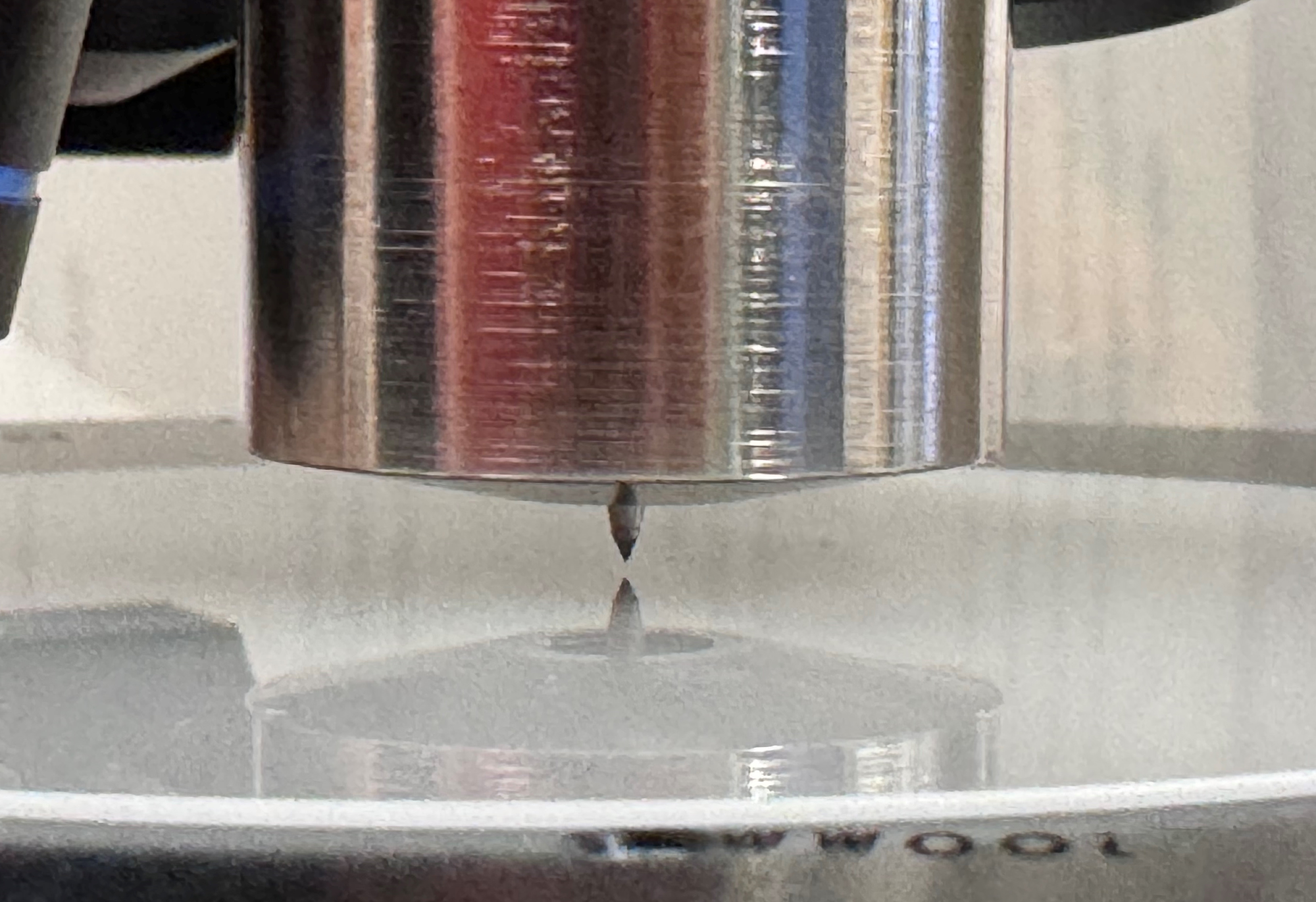
Figure 1. Diamond scribe mounted into the Zeta™-20 optical profiler objective turret. The scribe is centered in the holder, pointing down toward the wafer below. Image Credit: KLA Instruments™
Workflow Optimization
Sample preparation for electron microscopy, FIB and AFM often involves optical inspection and identification of the area of interest for alignment and understanding of the feature to be imaged and/or analyzed. The Zeta-20 combines optical imaging and 3D profiling with a high-resolution diamond scriber for marking the area of interest. Using Automated Optical Inspection (AOI), defects or features are first identified and categorized. The user can then select defects/features of interest and center them under the microscope with a single click of a button. Once the feature is centered under the microscope, a push button operation rotates the turret to the diamond scribe and pre-defined markings are then etched into the sample. These markings can be controlled for force (Figure 2), shape and dimensions. With a high magnification (≥ 50X) objective, marking can be achieved to micron-level lateral resolution.
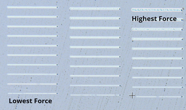
Figure 2. Scribe force test on silicon to determine optimum scribe force; the lowest force is at the bottom left, increasing to the maximum at the top right. Image Credit: KLA Instruments™
Case Study – Enabling and Accelerating FIB SEM Analysis
A glass wafer with an Indium Tin Oxide (ITO) film was inspected for defects on a Zeta-20 (Figure 3, Step 1) and select defects were marked with the built-in diamond scribe (Figure 3, Step 2), enabling localization of invisible features in the SEM. The wafer was loaded into a Zeiss Sigma™ 360 FE-SEM, and the area located in under 1 minute (Figure 3, Step 3). To distinguish whether the defect was on the surface or at the ITO/glass interface, the sample was FIB-milled (Figure 3, Step 4) in a Zeiss Crossbeam™ 550. The cross-sectional image (Figure 3, Step 5) confirmed that the defect was embedded on the surface and not at the interface.
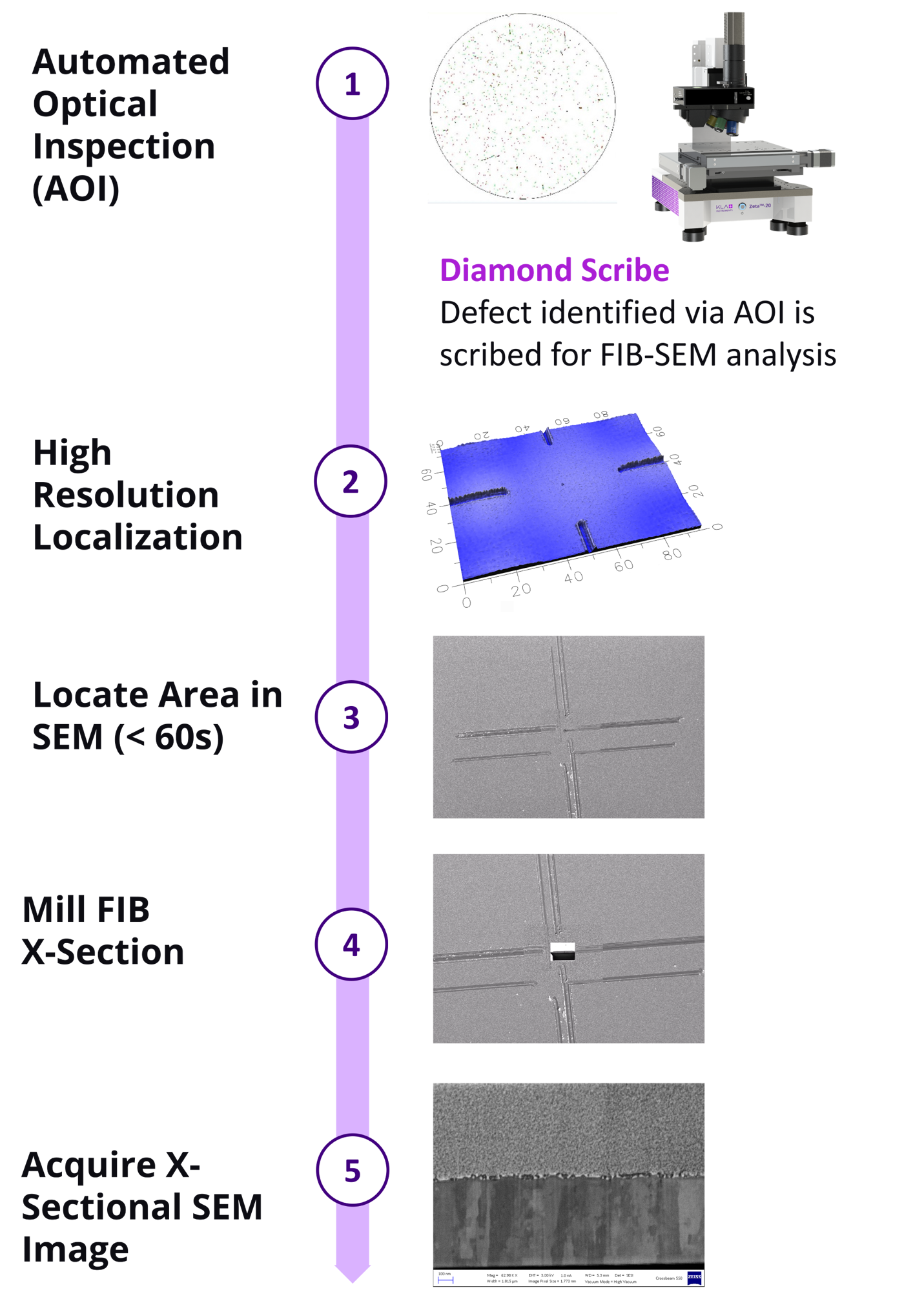
Figure 3. Sample preparation workflow for identifying, locating, marking and analyzing features of interest. Image Credit: KLA Instruments™
Case Study – Repeating Pattern
In memory and other devices, there are repeating patterns that may include hundreds of columns and rows (Figure 4, left). If a specific structure must be analyzed, then counting them can be time-consuming and fraught with uncertainty. Did the user land in the right area for analysis? To eliminate this uncertainty, once a feature is identified via optical inspection, it can be marked with the diamond scribe to quickly find the area of interest in the SEM or FIB SEM and land on it with confidence (Figure 4, right).
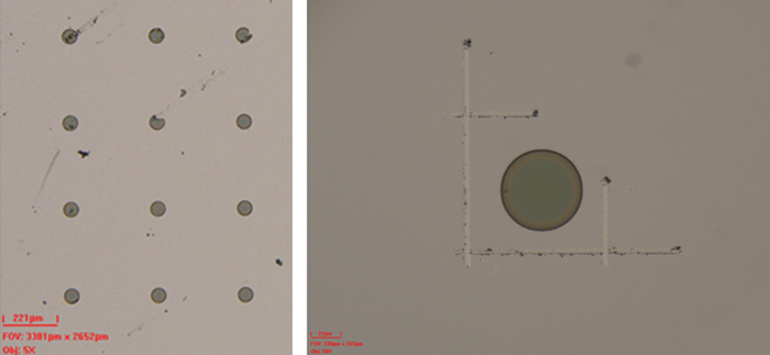
Figure 4. Repeating memory pattern (left) with an individual structure marked for further analysis (right). Image Credit: KLA Instruments™
Synergy of the Diamond Scribe with Automated Defect Detection
The diamond scribe capability is synergistic with the Automated Optical Inspection (AOI) capability of the Zeta Series systems. AOI is a powerful technique for scanning samples to find the location and size of defects. AOI is useful for (1) locating difficult-to-find isolated defects, (2) gathering statistical size distributions when many defects are present and (3) for Defect Review. Defect Review can include optically profiling the topography of the defect, using the diamond scribe to mark the location of defects for further study, and exporting a KLARF file of the defect location(s) for other uses, such as pick and place. Figure 5 illustrates two examples from a rich set of defect topographies that can be located with AOI.
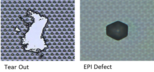
Figure 5. Examples of defects that can be located using the Zeta AOI defect detection application. Image Credit: KLA Instruments™
The AOI application generates lists of all defects found (the number of which can reach into the thousands and beyond) and allows for sorting them. Figure 6 illustrates how a particular defect in the defect list has been selected and then positioned in the FOV of the low magnification objective lens, ready for further optical analysis. A higher magnification lens is then selected and brought into place using the automated turret. Figure 7 illustrates measurements of the defect height and lateral dimension at higher optical magnification using ZDot™ technology.
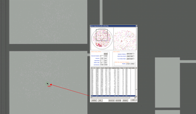
Figure 6. Defect Traceback of the Zeta AOI analysis capability. Image Credit: KLA Instruments™
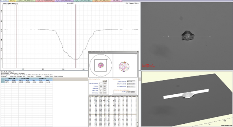
Figure 7. High resolution 3D topography of a defect located using AOI. Image Credit: KLA Instruments™
At this point, the synergy of diamond scribing, ZDot characterization, and AOI defect detection becomes apparent. The diamond scribe is switched into position and fiducial marks are scribed onto the sample. Additional defects can be selected from the AOI defect list and analyzed for their vertical and horizontal geometries and marked for later analytical analysis in a similar fashion.
Diamond Scribe Applications
The Zeta diamond scribe has found use in many different applications including marking locations for FIB sample preparation, SEM examination, and AFM imaging. It can be employed across various industrial and research laboratory environments in applications that include:
- Failure Analysis
- Material Analysis
- Defect localization
- Semiconductor
- Microscribe & circuit cleave
- Mark for FIB
- Mark defect located under photoresist for FIB SEM
- Microelectronics
- Bumps, pads, copper pillars on various wafer types
- Defect Inspection
- Mark sub-micron to large-sized features
- Mark mask and device defects located by Automated Optical Inspection (AOI)
- Optical
- Packaging
- Cosmetic and Appearance
- Scratches
- Regions of different color
- Regions of different texture
Materials spanning a wide range of hardness can be readily scribed with customizable scribe geometries and sizes. Together with programmable force control, materials exhibiting a wide range of mechanical hardness can be scribed. The high-resolution diamond scribe can also be an enabler for analysis/FA of films that are opaque to particle beams.
The integrated diamond scribe is useful for process development, to make new types of devices, improve existing components, as well as for failure analysis to understand why components don’t function as expected. A broad range of analysis techniques can take advantage of the scribe capability, including AFM, Auger, ellipsometry, ESCA, FIB, FTIR, Raman, SEM and many other analytical, optical and metrology techniques.
Summary
Micro- and nanoscale analysis requires high-resolution imaging, typically SEM or FIB SEM. Defects can be opaque to the electron beam, hidden under a top layer or protective coating and surrounded by featureless material. The KLA Instruments Zeta-20 can quickly mark areas of interest with a diamond scriber to achieve micron-level resolution for easy SEM location in ≤ 60 s. This technique can significantly increase the throughput for EM and FIB operations, allowing the user to concentrate on the analysis.

This information has been sourced, reviewed, and adapted from materials provided by KLA Instruments™.
For more information on this source, please visit KLA Instruments™.