This article introduces Park Systems' NX1, a compact high-resolution AFM optimized for stable atomic-scale imaging under ambient settings.
The NX1 combines a solid low-noise design, a Kovar-based AFM core body, and a precision XYZ tube scanner to provide an optimum solution for researchers studying atomic lattice imaging of crystalline and two-dimensional materials.
Introduction
Atomic force microscopy (AFM) has emerged as an essential method for nanoscale surface characterization, giving high-resolution data on surface shape, mechanical response, and functional properties across a wide range of materials.
AFM's ability to image both conducting and insulating samples makes it very useful for studying crystalline surfaces, two-dimensional materials, and other nanoscale structures that require local surface information.
Among the many AFM applications, atomic lattice imaging is one of the most demanding. Resolving periodic features at the atomic scale requires not only a sharp probe and optimal imaging conditions but also high mechanical stability, low noise, and minimal thermal drift.
These requirements become even more difficult in ambient conditions, when environmental vibration, temperature fluctuations, and instability in the tip-sample contact can obscure atomic-scale contrast.
To achieve reliable atomic lattice imaging, the AFM platform must be built to reduce mechanical noise while maintaining a stable tip-sample geometry during small-scan observations.
A rigid and compact mechanical structure, a reduced mechanical loop, and a low-drift scanner design are thus required for reproducible high-resolution imaging.
Park Systems created the NX1 to meet these needs by combining a low-noise mechanical architecture with a usable AFM methodology for high-resolution imaging in ambient environments.
Overview of NX1
The NX1 is Park Systems' compact high-resolution AFM, developed for stable atomic lattice imaging in ambient conditions.
The system was created in partnership with Prof. Franz J. Giessibl at the University of Regensburg, expanding on the Orpheus II concept for ambient AFM operation while using Park Systems' beam-bounce sensing and practical AFM process.
Its sturdy and compact architecture, reduced mechanical loop, Kovar-based AFM core body, and precision XYZ tube scanner ensure the stability needed for small-scan high-resolution measurements.
The device also accepts regular AFM probes and optional qPlus sensor sets for high-resolution AFM experiments. Figure 1 shows the NX1 with the SmartScanTM interface, which displays atomic-scale imaging results and real-time measurement signals during AFM operation.
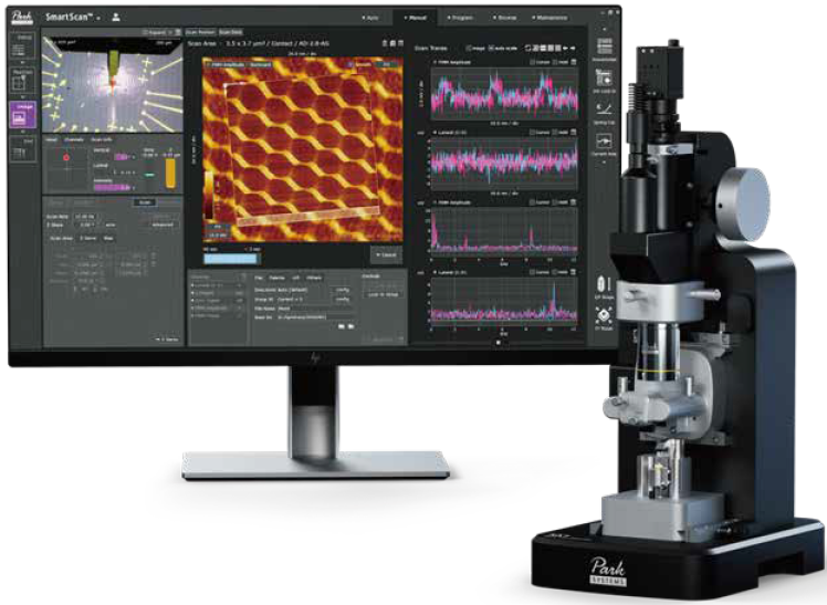
Figure 1. NX1 with the SmartScan™ operating interface. The monitor displays atomic-scale imaging results and real-time measurement signals during AFM operation. Image Credit: Park Systems
Key Feature 1: Optimized AFM Architecture for Atomic-Scale Imaging
For atomic lattice imaging, the AFM system must maintain a very stable tip-sample geometry throughout small-scan observations.
To meet this requirement, the NX1 incorporates a stiff and compact AFM architecture that reduces the mechanical loop between the probe and the sample. By reducing and strengthening this mechanical path, the device reduces mechanical noise while increasing stability for high-resolution imaging.
The NX1 features a Kovar-based AFM core body, a precision XYZ tube scanner, and a tungsten carbide stick-slip stage. Kovar, a nickel-cobalt ferrous alloy with a low thermal expansion coefficient, helps to reduce thermal drift in the AFM core body.
The XYZ tube scanner enables small-scan high-resolution imaging, while the stick-slip stage ensures accurate placement for approach and sample navigation. These components form the mechanical foundation for stable atomic-scale AFM observations.
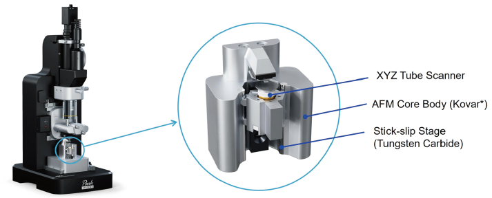
Figure 2. Optimized AFM architecture of NX1. The compact Kovar-based AFM core body, XYZ tube scanner, and tungsten carbide stick–slip stage are designed to support stable atomic-scale imaging. (* Kovar: nickel-cobalt ferrous alloy, Thermal Expansion Coefficient: 6 ×10⁻⁶ K-1). Image Credit: Park Systems
Key Feature 2: Exceptional Stability with Low Noise Floor and Reduced Thermal Drift
The stability of the AFM platform has a direct impact on the quality and reproducibility of atomic lattice imaging. Even minor vertical or lateral noise can distort the periodic contrast of atomic structures, particularly when imaging at scan sizes of a few nanometers.
The NX1 was developed to reduce mechanical noise and thermal drift as a result of its small, low-noise architecture.
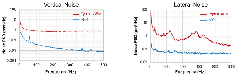
Figure 3. Noise floor comparison between NX1 and a typical AFM. NX1 shows reduced vertical and lateral noise for stable high-resolution imaging. Image Credit: Park Systems
Figure 3 shows that the NX1 reduces vertical and lateral noise by an order of magnitude compared to a normal AFM. The zero-scan vertical noise is decreased from 0.24 Å to 0.02 Å, while the zero-scan lateral noise is lowered from 1.40 Å to 0.04 Å.
This low noise level enables highly stable and reproducible atomic-resolution imaging, ensuring the measurement stability required to resolve atomic lattice structures in ambient circumstances.
Key Feature 3: Intuitive Optical Access and Laser Beam Alignment
While the NX1 is designed for high-resolution imaging, practicality remains a key consideration. The beam-bounce detection module is separated from the AFM core body, allowing for optical access and cantilever deflection detection while maintaining the AFM core's mechanical stability.
The NX1 detects cantilever motion using beam-bounce deflection sensing, which is highly sensitive.
A superluminescent diode (SLD) offers low-coherence illumination, reducing optical interference, while laser alignment knobs allow the laser beam to be aligned on the cantilever. The reflected beam is then centered on the PSPD through steering mirror alignment adjustments, making setup easier.
The device also includes an on-axis optical microscope for a direct view of the sample surface and an AFM probe.
This optical access enables users to pinpoint the region of interest and position the probe before performing high-resolution AFM measurements. Software-controlled LED illumination improves visibility across sample types, allowing for more efficient sample navigation and measurement preparation.
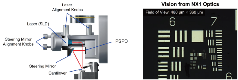
Figure 4. Laser beam alignment and optical vision of NX1. The laser beam alignment pathway enables cantilever deflection detection, while the on-axis optics provide a direct view of the sample surface. Image Credit: Park Systems
Key Feature 4: Easy Probe Exchange and Measurement Versatility
Probe handling is a key aspect of practical AFM operation, particularly for high-resolution measurements that need consistent probe positioning.
Pre-aligned probe chip carriers and kinematic mounting points in Park Systems' probe holder design help ensure consistent probe alignment and eliminate probe-handling difficulties.
The NX1 supports both standard AFM probe and optional qPlus sensor holder configurations, allowing users to choose the optimal sensor setup according to the measurement purpose.
The optional qPlus sensor holder is compatible with high-stiffness quartz tuning-fork sensors for measurements requiring increased sensitivity to short-range forces.
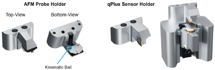
Figure 5. AFM probe holder and qPlus sensor holder for NX1. The system supports both standard AFM probes and optional qPlus sensors for high-resolution AFM measurements. Image Credit: Park Systems
Key Feature 5: Atomic Lattice and Moiré Imaging on Two-Dimensional Materials
Atomic lattice imaging is a vital tool for analyzing crystalline surfaces and two-dimensional material systems, as local lattice periodicity, crystalline order, and moiré superlattice structures provide valuable information about the sample.
To show NX1 performance in this application, four representative samples were chosen: MoS2 single crystal for LFM-based atomic lattice imaging on a layered two-dimensional semiconductor, highly oriented pyrolytic graphite (HOPG) as a reference material for FMM-based lattice imaging, and twisted bilayer graphene and WSe2 on graphene for multi-scale FMM imaging of moiré structures.
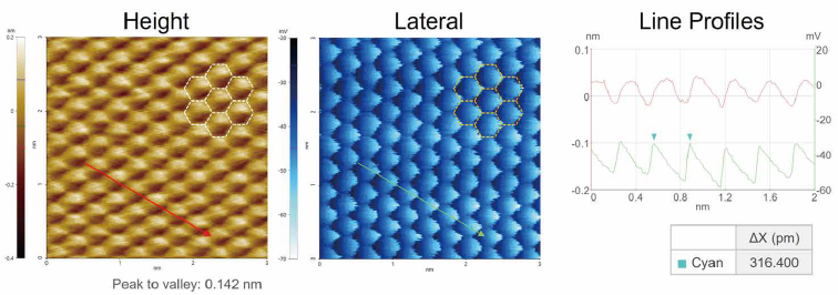
Figure 6. Atomic lattice imaging of MoS2 single crystal using NX1. Height and lateral signals measured by LFM clearly resolve the atomic lattice structure at a 3 nm scan size. The corresponding LFM measurement conditions were as follows: 256 × 256 pixels, scan rate of 16 Hz, and a scan size of 3 × 3 nm2. Image Credit: Park Systems
Figure 6 shows atomic lattice imaging of a MoS2 single crystal, a layered two-dimensional semiconductor with a hexagonal lattice structure. MoS2 was chosen to assess atomic periodicity in a typical non-graphite-based 2D crystal.
Lateral force microscopy (LFM) was used to measure the sample at a scan size of 3 nm, and the atomic lattice could be seen clearly in both height and lateral signals. The observed lattice spacing of 3.164 Å matches the reference lattice constant of MoS2, indicating a consistent atomic-scale measurement.
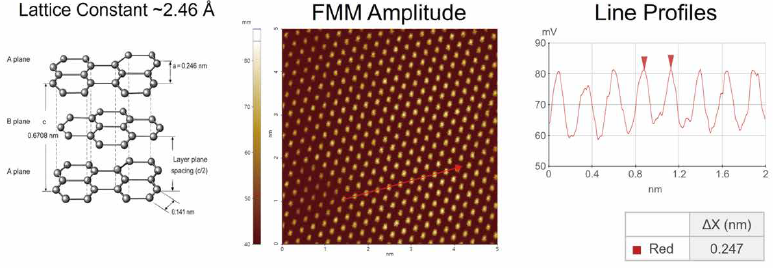
Figure 7. Atomic lattice imaging of HOPG using NX1. FMM amplitude imaging resolves the periodic lattice structure of graphite at a 5 nm scan size. The corresponding FMM measurement conditions were as follows: 512 × 512 pixels, scan rate of 12 Hz, and a scan size of 5 × 5 nm2. Image Credit: Park Systems
HOPG is commonly used as a reference material for atomic-scale AFM imaging due to its well-defined layered graphite structure and established lattice spacing. Figure 7 shows force modulation microscopy (FMM) amplitude imaging of HOPG at a 5 nm scan size, which resolves the periodic lattice structure of graphite.
The measured lattice spacing aligns with the graphite reference value, proving NX1's ability to obtain stable atomic lattice pictures using FMM.
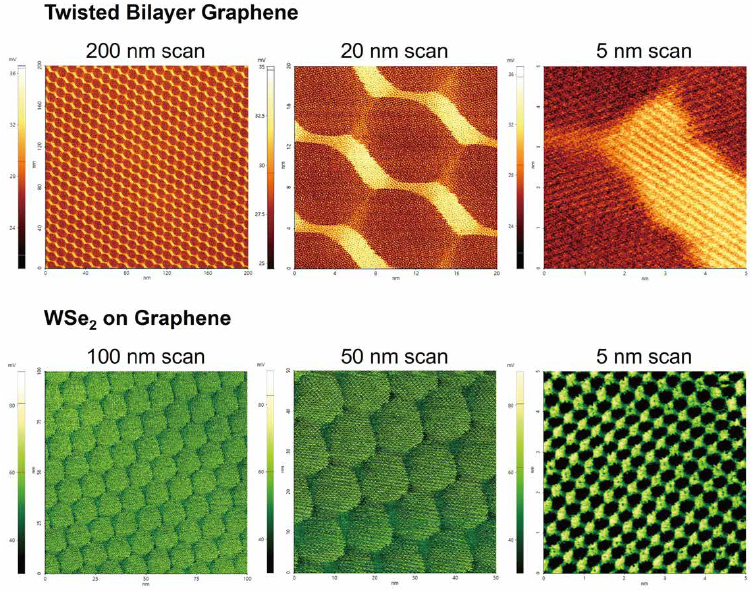
Figure 8. Multi-scale FMM imaging of twisted bilayer graphene and WSe2 on graphene using NX1. Moiré patterns are observed at larger scan sizes, while atomic lattice features are resolved at smaller scan sizes. The corresponding FMM measurement conditions were as follows: 512 × 512 pixels and scan rates of 12 Hz for twisted bilayer graphene and 8 Hz for WSe2 on graphene. Scan sizes are indicated in each image. Image Credit: Park Systems
Beyond direct atomic-lattice imaging, the NX1 allows for multi-scale imaging of moiré features in two-dimensional material systems. Twisted bilayer graphene and WSe2 on graphene were chosen as exemplary moiré systems because they had periodic patterns at many length scales.
Twisted bilayer graphene produces a moiré superlattice due to rotational misalignment of the graphene layers, whereas WSe2 atop graphene produces moiré patterns because of lattice mismatch between the two materials.
Figure 8 shows moiré patterns at larger scan sizes, whereas atomic lattice features are resolved as the scan size is reduced, illustrating NX1's capacity to image 2D material systems from the nanoscale to the atomic scale.
Conclusions
Advances in AFM technology continue to improve surface characterization at ever-smaller length scales, making reliable atomic-scale imaging an essential capability for current materials research.
Park Systems' development of the NX1 demonstrates its dedication to providing a practical high-resolution AFM platform for researchers studying atomic lattices under ambient conditions.
The NX1's sturdy and compact low-noise architecture, minimal mechanical loop, Kovar-based AFM core body, precision XYZ tube scanner, and optimized optical/probe process are all geared toward enabling stable and reproducible high-resolution measurements.
The atomic lattice and moiré imaging results presented in this article show that the NX1 can image crystalline surfaces and two-dimensional material systems at the atomic scale under ambient conditions.
Acknowledgments
Produced using materials originally authored by Jay Son from Park Systems.
This information has been sourced, reviewed, and adapted from materials provided by Park Systems.
For more information on this source, please visit Park Systems.