By coupling a high-mobility semiconductor to a piezoelectric substrate, researchers tested whether surface acoustic waves could deliver stable microcurrents without conventional rectifier circuitry.
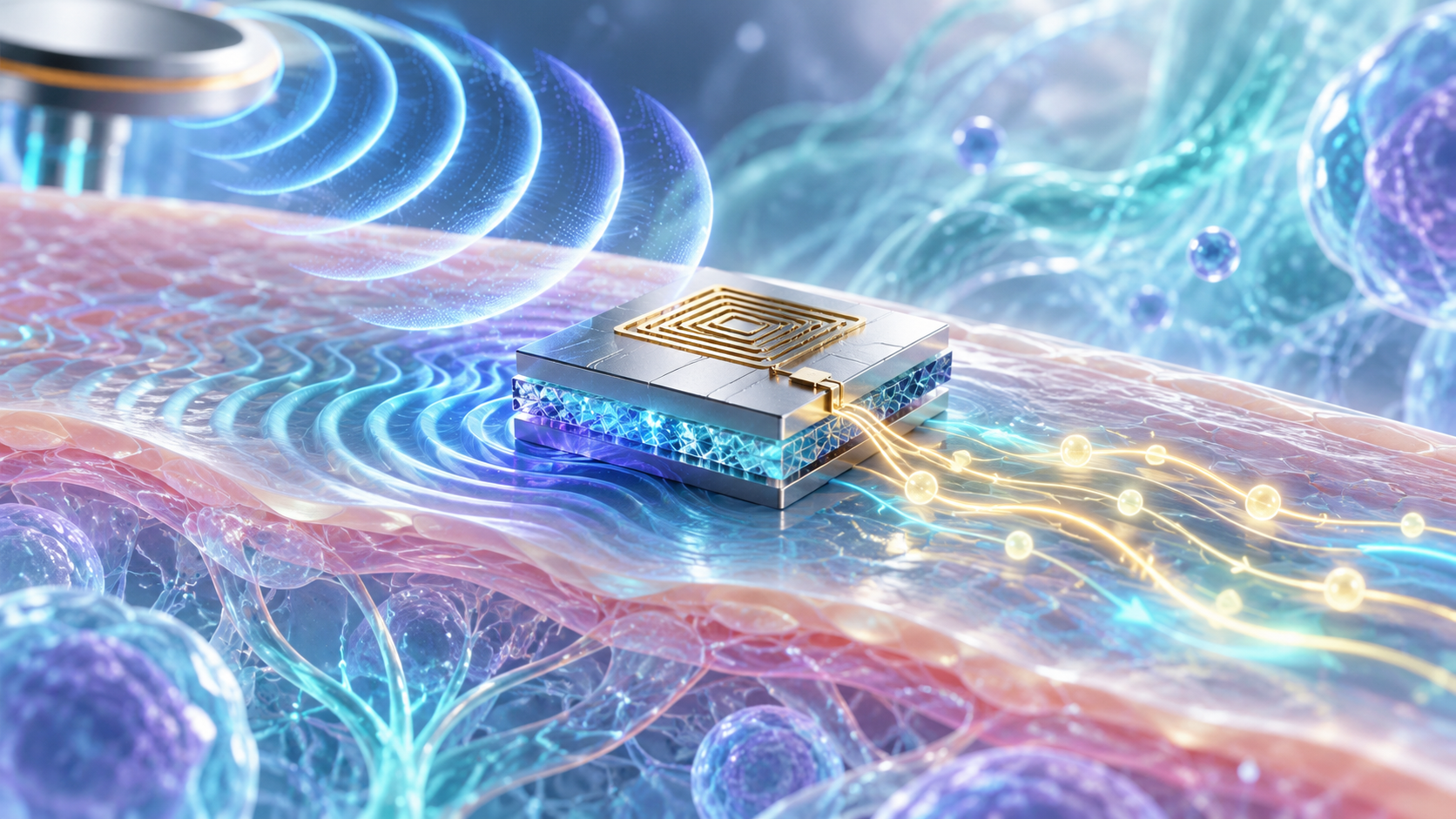
Paper: Wireless acoustic-driven current source achieving nanoampere-level at millimeter-scale. AI-generated abstract conceptual image created using ChatGPT/OpenAI
A recent study in Nature Communications presents an acoustically driven current source that generates tunable electrical currents ranging from 1.22 nA to 25.46 μA under direct RF excitation and can also be powered wirelessly. The researchers combined a high-mobility InSb semiconductor with a lithium niobate piezoelectric substrate to convert radiofrequency energy into direct current through the acoustoelectric effect.
Addressing the Need for Wireless Nanoampere Current Sources
Microcurrent stimulators are used in neural modulation, tissue regeneration, and pain therapy. These systems require stable, low-amplitude currents because current variations can affect their performance. Wireless sensor networks and radiofrequency signal-processing platforms also require precise current sources. Conventional circuits can generate nanoampere-level currents with good stability, but they generally rely on wired power. Wireless power transfer removes this limitation, but conventional systems often require several components, including antennas, matching networks, rectifiers, and filtering circuits. At high RF power, conventional diode or transistor rectifiers can be much simpler and implemented in compact silicon circuits.
The researchers explored the acoustoelectric (AE) effect as another method for generating current. Radiofrequency energy excites surface acoustic waves (SAWs) on a piezoelectric substrate. These waves generate an acoustic field that interacts directly with charge carriers in a semiconductor, producing a continuous direct current. This approach removes the need for separate rectification components and could simplify device integration.
Practical AE current sources face several challenges. Researchers must integrate high-quality semiconductors with strongly piezoelectric materials such as lithium niobate while maintaining effective acoustic-carrier interaction. The team developed a semiconductor-piezoelectric heterostructure that strengthens this interaction and provides a stable current over a wide, tunable range.
Engineering the InSb-LiNbO3 Acoustoelectric Platform
The current source uses a SiOx/InSb/In0.6Al0.4Sb heterostructure on a 128°YX LiNbO3 substrate. Interdigital transducers (IDTs) excite the LiNbO3 substrate, generating surface acoustic waves. The waves create a piezoelectric potential that interacts with electrons in the InSb layer. That interaction moves the carriers and produces direct current.
The In0.6Al0.4Sb buffer layer improves the crystalline quality of the InSb active layer and helps address the lattice mismatch between InSb and LiNbO3. The SiOx layer protects the structure during annealing and limits unwanted Sb out-diffusion. Because the buffer layer has high electrical resistance, it does not substantially screen the SAW-generated piezoelectric field. Measurements showed stronger InSb diffraction peaks and narrower peak widths after the buffer layer was introduced.
Hall measurements showed that the heterostructure with the buffer layer achieved a carrier mobility of 1667 cm² V-¹ s-¹, a sheet carrier density of 6.94 × 10¹¹ cm-², and a sheet conductivity of 1.9 × 10⁻⁴ S at room temperature. The InSb active layer measured 250 nm in thickness, while the compact active region measured about 2.3 mm × 0.5 mm × 0.5 mm. That quoted size covers the active region, including the IDTs and multilayer film, rather than the receiving antenna or external RF equipment.
The researchers also developed a coupling-of-modes model that incorporated the AE effect. The model connected acoustic transmission characteristics with current generation and closely reproduced the experimental results. It helped the team refine the device structure and identify conditions that improve acoustic-carrier interaction.
Four Orders of Current Control and Long-Term Stability
Across the frequency sweep, the AE current follows the acoustic transmission response, peaking at 434.75 MHz, where the acoustic intensity is highest. As RF input power increases, stronger acoustic waves transfer more energy to the semiconductor carriers, increasing the output current. The experimental results match the predictions from the coupling-of-modes model.
Researchers varied RF input power from 5 μW to 200 mW during wired measurements. The average output current showed a near-linear relationship on logarithmic axes, giving R² = 0.999. Under these wired test conditions, the device covers an output range of 1.22 nA to 25.46 μA, spanning four orders of magnitude. It also generates a maximum reliable output voltage of about 335 mV. Short tests across several input powers kept the reported current accuracy below 3%. At 10 mW and 25 °C, a 12-hour test produced an average current of 1.543 μA with a standard deviation of 4.82 nA. The authors report a ±1% variation in current at 10 mW, using the experiment's average current as the reference value. At high input powers, Joule heating becomes an important limitation. Heat shifts the IDT resonant frequency and reduces current linearity. Excessive heating can also damage the dielectric layer and electrodes.
The researchers propose better thermal management, including the possible use of LiNbO3 thin films on silicon substrates. Output impedance remains approximately 10.5 kΩ from 20 Hz to 100 kHz. The paper reports that this impedance is lower than that of conventional voltage-controlled current sources and is best suited to loads below about 1 kω if the loading error is to remain under 10%. Above 100 kHz, the impedance falls as the device shows a capacitive response. Its current response also changes predictably with temperature between −20 and 40 °C, providing a basis for temperature-compensation methods.
The device can generate current without a direct electrical connection to the RF source. Receiving antennas capture the RF signal and excite the acoustic device, which converts the resulting acoustic energy into DC through the AE effect. The researchers achieved stable wireless operation at distances below 60 cm using RF powers of 10 and 100 mW. Current fell quickly with distance: at 30 cm it was below 5% of the wired baseline. The paper also reports that antenna orientation, multipath fading, and environmental reflections can disturb the power-current relationship in practical settings. The team tested other transducer layouts to recover some of the current lost during wireless operation. At 10 dBm and a 10 cm wireless distance, a two-IDT array increased the average current by about 113%, whereas a unidirectional transducer design increased it by about 43% relative to the conventional IDT delay line.
The researchers tested the platform in a rat full-thickness skin defect model. Wireless low-intensity electrical stimulation showed a trend toward faster wound closure. The authors describe the result as preliminary and say more biological validation is needed. The study involved 24 male Sprague-Dawley rats, divided into a control group and groups receiving 10 or 20 μA of stimulation over 11 days. Relatively low RF-to-DC conversion efficiency limits the current output. Generating higher stimulation currents would require larger receiving antennas or better overall energy-conversion efficiency. The Discussion also flags RF exposure as a practical constraint. At the 430 MHz continuous power-density limit cited by the authors, they estimate that obtaining even 10 μA would require an impractically large receiving antenna.
Toward Wireless Nanoampere-Scale Electronics
This study demonstrates another way to generate tunable nanoampere-to-microampere currents, with wireless excitation tested separately. Surface acoustic waves drive charge carriers directly without conventional rectifier circuits. Under wired RF excitation, the active device region delivered 1.22 nA to 25.46 μA and measured about 2.3 mm × 0.5 mm × 0.5 mm. Wireless tests showed that the same current-source concept can operate through an antenna link.
The results suggest potential applications in bioelectronic interfaces and low-voltage, low-impedance electronics, but the paper primarily presents the work as a demonstration of the AE conversion mechanism. Its RF-to-DC conversion efficiency remains orders of magnitude lower than that of conventional rectification circuits. The roughly 10.5 kΩ output impedance and limited output voltage, in the tens to hundreds of millivolts, also make direct use with high-impedance silicon logic difficult without extra voltage boosting. The researchers identify thermal management, antenna design, electromechanical coupling, semiconductor mobility, and system-level design as areas for more work.
The work shows that acoustoelectric conversion can provide a compact route for wireless current generation. The authors present it as a rectifier-free demonstration rather than a near-term replacement for efficient conventional rectifiers. Higher conversion efficiency, better heat removal, and improved antenna design are still needed before the technology can support broader practical wireless-power and biomedical applications.
Disclaimer: The views expressed here are those of the author expressed in their private capacity and do not necessarily represent the views of AZoM.com Limited T/A AZoNetwork the owner and operator of this website. This disclaimer forms part of the Terms and conditions of use of this website.