Among the most extensively researched nanomaterials in modern science are graphene, a two-dimensional lattice of sp2-bonded carbon, and carbon nanotubes (CNTs), the one-dimensional cylinders produced when a graphene sheet is rolled upon itself.
Both materials possess optical, electrical, mechanical, and thermal characteristics that exhibit high sensitivity to structure, defect density, layer or wall number, and local chemical environment.
This article outlines how UV-Visible-NIR transmission and reflectance microspectroscopy, UV microscopy, photoluminescence microspectroscopy, and Raman microspectroscopy were conducted using a single microspectrophotometer on micron-scale sample regions.
The microspectrophotometer was employed for the non-destructive characterization of graphene and carbon nanotube samples, demonstrating its utility for research, quality control, and process development.
Introduction
Graphene is a two-dimensional carbon form arranged in layers only one atom thick, with the atoms densely packed in a regular hexagonal pattern. Mathematically, the sheet can be considered an infinitely large aromatic molecule, producing new electronic phenomena that arise from its distinctive physical and electronic structure.
Thanks to its properties, graphene can potentially serve as the foundation for numerous emerging applications and gadgets.
Carbon nanotubes (CNTs) are structures formed when a graphene sheet is rolled at a specific angle to form a cylinder. An individual CNT is considered a one-dimensional material, unlike two-dimensional graphene. The angle at which the sheet is rolled, known as its chirality, directly affects the nanotube's electronic characteristics.
Nested tubes consisting of several concentric graphene layers are known as multi-walled nanotubes.
Carbon nanotubes consist of extensive networks of sp2 carbon-carbon. These bonds are responsible for the exceptional tensile strength of individual CNTs and also contribute to the distinctive optical, mechanical, electrical, and thermal characteristics that make CNTs of interest across numerous fields.
Since both graphene and carbon nanotubes possess characteristic absorbance, photoluminescence, and Raman spectral signatures, optical microspectroscopy is a valuable, non-destructive method for their examination. This approach enables researchers and engineers to investigate and “tune” the properties of newly developed carbon nanostructures.
Microspectroscopy is widely used in quality control to assess structural imperfections, detect contaminants, determine layer or wall thickness, and verify that the intended optical and electronic attributes have been achieved.
CRAIC Technologies has created a variety of complementary spectroscopic techniques that can be integrated into a single instrument for examining graphene, CNTs, and other one-, two-, and three-dimensional structures.
The 2030PV PRO™ UV-VIS-NIR microspectrophotometer (Figure 1) may be configured for transmission, reflectance, photoluminescence, and Raman spectroscopy and imaging. This configuration allows a single micron-scale sample region to be examined using multiple complementary methods.
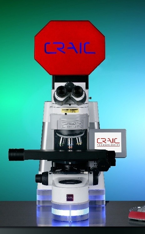
Figure 1. The 2030PV PRO™ UV-VIS-NIR microspectrophotometer from CRAIC Technologies. This instrument can be configured for transmission, reflectance, photoluminescence, and Raman spectroscopy and imaging. Image Credit: CRAIC Technologies
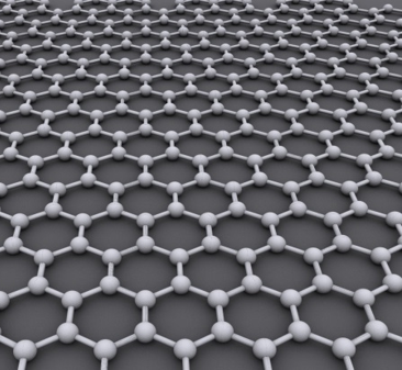
Schematic representation of a single graphene layer, a hexagonal lattice of sp2-bonded carbon atoms. Image Credit: AlexanderAIUS - own work, License CC BY-SA 3.0, https://en.wikipedia.org/wiki/Graphene#/media/File:Graphen.jpg
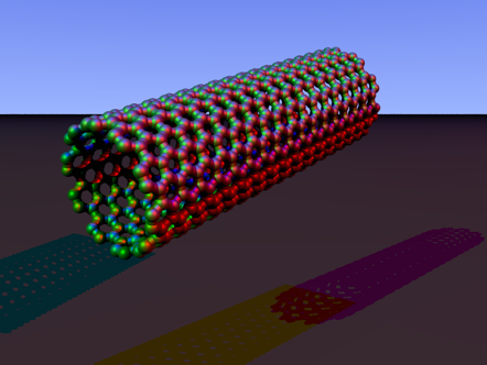
A single-walled carbon nanotube, formed by rolling a graphene sheet into a seamless cylinder. Image Credit: Arnero - own work, Public Domain, https://commons.wikimedia.org/w/index.php?curid=3153687
UV-Visible-NIR Microspectroscopy
Transmission microspectroscopy across the ultraviolet, visible, and near-infrared regions has demonstrated considerable effectiveness for the characterization and identification of both graphene and carbon nanotubes.
Since sample preparation is relatively straightforward for both materials, transmission microspectroscopy has become a dependable and routine approach for evaluating composition, purity, oxidation state, and structural consistency.
Graphene: Oxidation State and Layer Number
Graphene oxide displays a characteristic absorption maximum at 230 nm associated with the π-π* transition of the aromatic C-C bond, along with a shoulder near 300 nm resulting from n-π* transitions of the C=O bond. Since these deep-UV characteristics are indicative of oxidation, transmission microspectra collected within this area are especially useful for differentiating pristine from oxidized graphene.
Transmission microspectroscopy is also ideally suited for the non-destructive determination of layer number. Pristine graphene absorbs around 2.29% of incident light for each layer within the visible-NIR region.
Figure 2 presents transmission microspectra obtained from graphene samples of increasing thickness, corresponding to 1, 2, 3–5, and 6–8 layers at the sampled areas. The systematic reduction in transmission as the layer count increases, particularly evident in the deep-UV region, directly highlights this layer-additive absorption behavior.
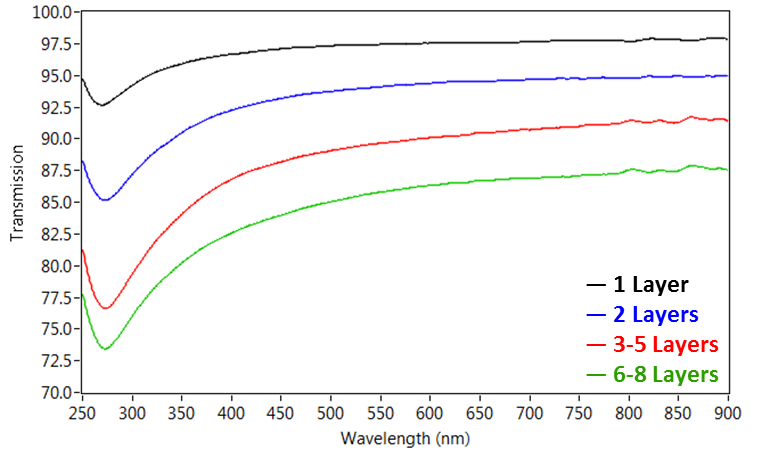
Figure 2. Transmission microspectra of single, dual, and multi-layered graphene samples, illustrating the change in transmission in the deep-UV region with increasing graphene layer count (1, 2, 3–5, and 6–8 layers). Image Credit: CRAIC Technologies
As layer number further increases, interference patterns become visible within the reflectance spectrum, allowing conventional thin-film thickness techniques to be employed. Figure 3 presents absolute reflectance microspectra for single- and multiple-layer graphene. The shift and reshaping of interference peaks directly correspond to sample thickness.
By integrating graphene optical constants with the Fresnel equations, the algorithms in CRAIC FilmPro™ software can be used to quantitatively determine graphene film thickness from these interference spectra.
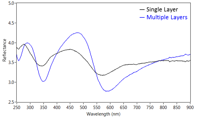
Figure 3. Absolute reflectance microspectra of single- and multiple-layer graphene, illustrating the change in interference peaks with sample thickness. Image Credit: CRAIC Technologies
Carbon Nanotubes: van Hove Singularities
Some of the most diagnostic optical absorptions in single-walled carbon nanotubes originate from the ν1-c1, ν2-c2, and higher electronic transitions, also referred to as van Hove singularities.
These transitions produce sharp, well-resolved features in the absorption spectrum. Since these transitions shift systematically with CNT structure, the resulting optical signatures can be utilized to determine tube type, purity, and structural properties.
Pure, single-walled carbon nanotubes display a pronounced absorbance maximum at 280 nm attributable to the CNT itself. The van Hove transitions occur well into the near-infrared, at around 1240 nm for the ν1–c1 (S11) transition and 700 nm for the ν2–c2 (S22) transition in isolated, pure material.
Figure 4 illustrates transmission microspectra of aggregated single-walled CNT material, dropcast on a quartz slide from an acetone suspension. While the characteristic 280 nm CNT peak remains visible, the van Hove transitions are red-shifted and broadened relative to their positions in isolated tubes.
This change occurs because the dispersion process produces a network of CNTs held together by van der Waals contacts.
Consequently, the precise wavelength of these shifted peaks can be used to evaluate how strongly the aggregated nanotube bundles are bound to one another, providing a straightforward, non-destructive indication of dispersion quality.
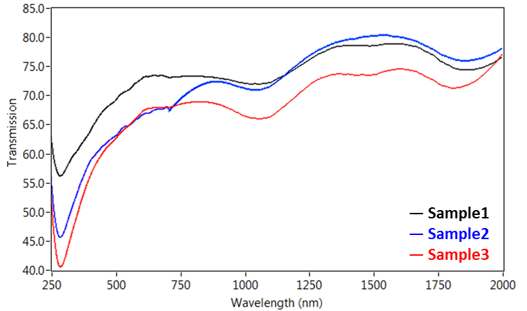
Figure 4. Transmission microspectra of single-walled carbon nanotubes dropcast on a quartz slide from an acetone suspension, showing peaks at approximately 280, 1050, and 1850 nm across three samples. Image Credit: CRAIC Technologies
Ultraviolet Microscopy
Although conventional visible-light microscopy is valuable for general sample examination, ultraviolet microscopy offers a rapid and efficient approach for verifying CNT location in a sample.
By using a UV-capable camera for imaging together with a bandpass filter tuned to an absorption peak of the material (e.g., 280 nm for single-walled CNTs), the spatial distribution of nanotube material can be quickly and clearly verified, as demonstrated in Figure 5.
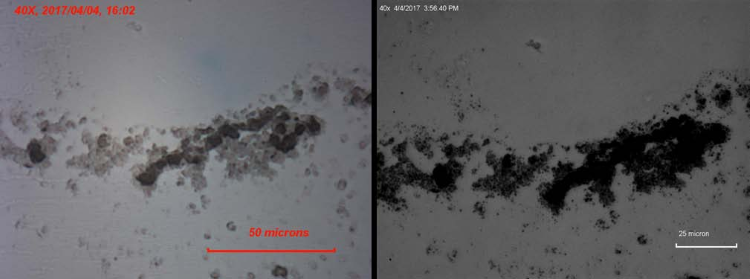
Figure 5. Standard visible images (left) and corresponding UV images at 280 nm (right) of single-walled CNT material dropcast on a quartz slide from an acetone suspension, at two representative sample locations. UV contrast at the CNT absorption maximum confirms nanotube location and distribution. Image Credit: CRAIC Technologies
Photoluminescence Microspectroscopy
When excited by a photon whose energy corresponds to the S22 transition, single-walled carbon nanotubes emit near-infrared light. The absorbed photon elevates the CNT into an excited state, which subsequently relaxes through the S11 transition; the emitted photon has an energy corresponding to this S11 transition.
Since this emission’s wavelength is highly sensitive to CNT structure, photoluminescence microspectroscopy offers an additional, complementary approach to structural identification. This capability is not directly available for graphene, which, in its pristine form, does not possess a comparable direct-bandgap emission pathway.
Importantly, the photoluminescence of single-walled CNTs is linearly polarized along the long axis of the tube. This characteristic makes it possible to monitor the orientation of individual nanotubes or nanotube bundles without extra sample preparation or equipment.
Raman Microspectroscopy
Raman microspectroscopy is a particularly effective technique for both graphene and carbon nanotubes, as the vibrational spectrum acquired represents the specific bonds present and is sensitive to the local structural environment.
Since every atomic bond possesses a vibrational frequency determined by the masses of the bonded atoms and the bond strength between them, complex carbon structures produce distinctive peaks that collectively create an easily recognizable spectral “fingerprint.”
This sensitivity is particularly useful for one- and two-dimensional materials, where the sampling region is restricted by the dimensions of the laser spot. As a result, local variations in structure and environment are resolved at the micron scale.
For graphene-based materials, three distinctive bands are generally detected: the D-peak near 1360 cm-1, the G-peak near 1600 cm-1, and the 2D-peak near 2700 cm-1. The G-peak results from carbon-carbon bond stretching, whereas the D-peak indicates disorder or contaminants within the carbon framework.
Consequently, the D-peak can serve as a direct measure of sample disorder. The 2D-peak is common to all graphitic samples, and its intensity, width, and position can be leveraged to ascertain the number of layers present.
The same D- and G-band properties are likewise diagnostic in carbon nanotube samples, reflecting the analogous sp2 bonding network. In each case, the precise vibrational band frequency is affected by the local environment, including substrate, residual solvent, and localized defects.
Figure 6 presents a comparison of Raman spectra obtained from pristine graphene, oxidized graphene, and carbon nanotube samples. The D-, G-, and 2D-peaks are distinctly resolved in all three samples.
Oxidized graphene exhibits a substantially more intense D-peak than pristine graphene, in agreement with the defects and disruption of the sp2 lattice caused by oxidation, while pristine graphene maintains a relatively sharp and strong 2D-peak.
The additional band appearing near 2205 cm-1 in the graphene spectra originates from the substrate on which the samples were mounted rather than from the graphene itself. Therefore, this band should not be interpreted as a characteristic of the sample.
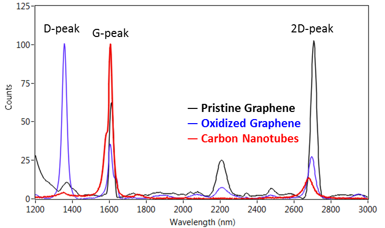
Figure 6. Raman spectra of graphene and carbon nanotube samples. The D-, G-, and 2D-peaks are clearly visible in all three samples. The additional band near 2205 cm-1 is due to the substrate on which the graphene samples were mounted. Image Credit: CRAIC Technologies
Instrumentation
CRAIC develops and manufactures UV-visible-NIR range microspectrometers for a broad range of applications, integrating multiple spectroscopic methods into a single instrument that can measure spectra from micron-scale sample regions.
Figure 7 illustrates the optical diagram of a microspectrophotometer set up for transmission microspectroscopy. Light is focused onto the sample, while the transmitted light is gathered and imaged onto the entrance aperture of the spectrophotometer.
Since the entrance aperture is mirrored, an image of the aperture is superimposed over the sample measurement region instantaneously. This arrangement enables rapid and straightforward alignment between the imaging and spectroscopic optical paths.
Raman microspectroscopy needs a somewhat different optical configuration, as illustrated in Figure 8. In this configuration, an excitation laser is focused onto the sample by the incident illumination path. The resulting Raman-scattered (Stokes) light is gathered and imaged onto the entrance aperture of the spectrophotometer, where the Raman microspectra™ is recorded.
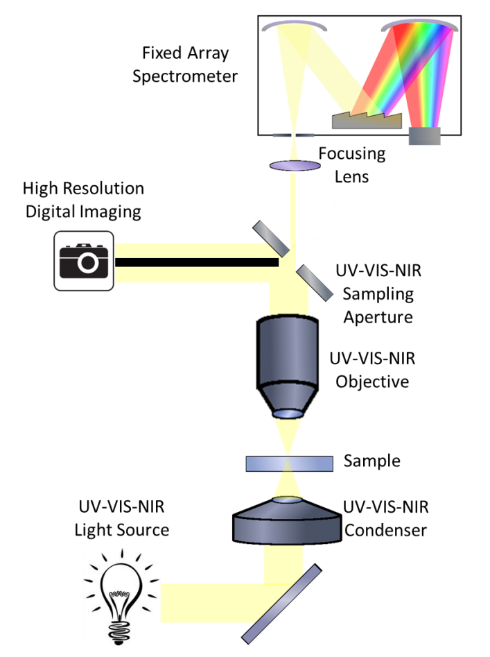
Figure 7. Optical diagram of a microspectrophotometer configured for UV-VIS-NIR transmission microspectra. Image Credit: CRAIC Technologies
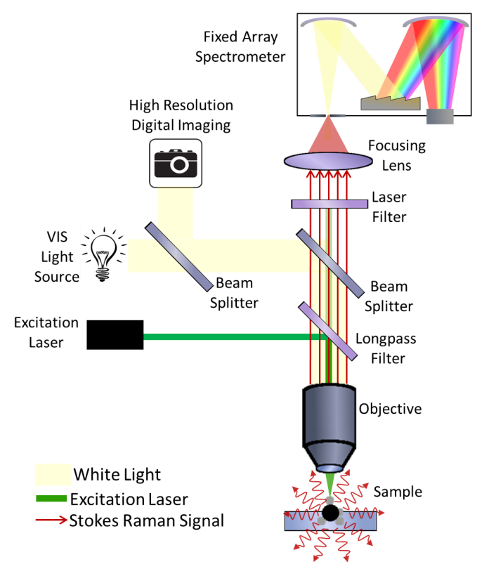
Figure 8. Optical diagram of a microspectrometer configured for Raman microspectra. Image Credit: CRAIC Technologies
In addition to transmission and Raman microspectroscopy, the same system provides UV and NIR imaging alongside conventional color imaging. It can also be configured for reflectance, photoluminescence, and polarization microspectroscopy, small-spot thin-film thickness measurement, kinetic spectroscopy, and 5D spectral surface mapping. This enables a single micron-scale sample region to be characterized from several complementary perspectives without requiring a change of tools.
Conclusion
Collectively, transmission and reflectance UV-Visible-NIR microspectroscopy, UV microscopy, photoluminescence microspectroscopy, and Raman microspectroscopy form a complementary, non-destructive toolkit for investigating the structural and electronic characteristics of graphene and carbon nanotubes.
UV-Vis-NIR transmission spectroscopy determines oxidation state and layer number in graphene while revealing the van Hove electronic structure and aggregation state of carbon nanotubes. Reflectance interferometry allows independent, quantitative measurements of graphene film thickness.
UV microscopy provides a fast means of locating CNT material within a sample. Photoluminescence microspectroscopy contributes structural and orientational sensitivity distinctive to semiconducting CNTs. Raman microspectroscopy provides a vibrational fingerprint shared by both materials and is sensitive to disorder, defect density, and layer number.
Since a single micron-scale microspectrophotometer platform can be used to conduct all these methods, scientists and quality-control engineers can readily transition between complementary measurements on the same sample region. This capability supports both fundamental investigations of these carbon nanomaterials and the practical requirements associated with process development and quality assurance.
References and Further Reading
- Mak, K. F., et al. (2012) Optical spectroscopy of graphene: From the far infrared to the ultraviolet, Solid State Communications, 152(15), pp. 1341–1349. DOI:10.1016/j.ssc.2012.04.064. https://www.sciencedirect.com/science/article/abs/pii/S0038109812002700.
- Bonaccorso, F., et al. (2010). Graphene photonics and optoelectronics. Nature Photonics, 4(9), pp.611–622. DOI:10.1038/nphoton.2010.186. https://www.nature.com/articles/nphoton.2010.186.
- Nikolaenko, A.E., et al. (2010). Carbon Nanotubes in a Photonic Metamaterial. Physical Review Letters, 104(15). DOI:10.1103/physrevlett.104.153902. https://journals.aps.org/prl/abstract/10.1103/PhysRevLett.104.153902.

This information has been sourced, reviewed, and adapted from materials provided by CRAIC Technologies.
For more information on this source, please visit CRAIC Technologies.